|
|
PDF NCP1501 Data sheet ( Hoja de datos )
| Número de pieza | NCP1501 | |
| Descripción | Dual Mode PWM/Linear Buck Converter | |
| Fabricantes | ON Semiconductor | |
| Logotipo | ||
Hay una vista previa y un enlace de descarga de NCP1501 (archivo pdf) en la parte inferior de esta página. Total 14 Páginas | ||
|
No Preview Available !
NCP1501
www.DataSheet4U.com
Dual Mode PWM/Linear
Buck Converter
The NCP1501 is a dual mode regulator that operates either as a
PWM Buck Converter or as a Low Drop Out Linear Regulator. If a
synchronization signal is present, the NCP1501 operates as a current
mode PWM converter with synchronous rectification. The
synchronization signal allows the user to control the location of the
spurious frequency noise generated by a PWM converter. Linear mode
is active when a synchronization signal is not present. The NCP1501
configuration allows an efficient high power operation and low noise
during system sleep modes.
Features
• Synchronous Rectification for Higher Efficiency in PWM Mode
• Linear Mode Operation for Low Noise Output at Low Loads
• Integrated MOSFETs and Feedback Circuits
• Cycle−by−Cycle Peak Current Limit of 800 mA (typ)
• Automatic Switching Between PWM and Linear Mode
• Operating Frequency Range of 500 to 1000 kHz
• Optimized for Ceramic Capacitors and Low Profile Inductors
• Thermal Limit Protection
• Built−in Slope Compensation for Current Mode PWM Converter
• Fixed Output Voltages of 1.05 V, 1.35 V, 1.57 V, 1.8 V
• Shutdown Current Consumption of 0.2 mA
• Internal Soft Start
• Transistor Count: 3500
• Pb−Free Package is Available
Typical Applications
• Cellular Phones
• PDAs
• Pagers
• Supplies for DSP Cores
• Portable Applications
Vout
10 m
L 10 mH
COUT
1 SHD CB0 8
2 SYN CB1 7
3 VO
4 LX
GND
Vin
NCP1501
6
5
Vbat
10 m CIN
http://onsemi.com
MARKING
DIAGRAM
8
1
Micro8E
(MSOP−8)
DM SUFFIX
CASE 846A
8
1501
AYW
1
1501= Device Code
A = Assembly Location
Y = Year
W = Work Week
PIN CONNECTIONS
SHD
SYN
VO
LX
1
2
3
4
(Top View)
8 CB0
7 CB1
6 GND
5 Vin
ORDERING INFORMATION
Device
Package
Shipping†
NCP1501DMR2
Micro8 4000/Tape & Reel
NCP1501DMR2G Micro8 4000/Tape & Reel
(Pb−Free)
†For information on tape and reel specifications,
including part orientation and tape sizes, please
refer to our Tape and Reel Packaging Specifications
Brochure, BRD8011/D.
Figure 1. Typical Applications Circuit
© Semiconductor Components Industries, LLC, 2004
March, 2004 − Rev. 7
1
Publication Order Number:
NCP1501/D
1 page 
NCP1501
DETAILED OPERATING DESCRIPTION
www.DataSheet4U.com
The Buck regulator is a synchronous rectifier PWM
regulator with integrated MOSFETs. This regulator has an
LDO function for low power modes to conserve power and
lower ripple voltage associated with PFM mode. The
NCP1501 does not contain an internal oscillator for the
switching mode. The Dual PWM/LDO mode is an exclusive
Patent Pending circuit.
The PWM clock is generated via an external clock signal
on the Synchronization pin. The operating frequency range
for the PWM is 500 kHz to 1000 kHz. The output current of
the PWM is typically 100 mA with a guarantee of over
300 mA for the 2.7 to 5.2 input voltage range.
If a synchronization pulse is not present, the NCP1501
changes into the LDO mode. The LDO function assures the
user of an extremely low output ripple voltage and greatly
reduced quiescent current when the users system is in a sleep
mode. Internally to the NCP1501, the Synchronization pin
has a pull down resistor to force the part into LDO mode
when a clock signal is not present. To place the NCP1501 in
LDO mode, the user must set the Synchronization pin low.
The LDO mode guarantees an output in excess of 50 mA.
Pins CB0 and CB1 control the output voltage selection.
The four voltages are 1.05 V, 1.35 V, 1.57 V, 1.8 V. CB0
contains a pull down resistor and CB1 contains a pull up
resistor internal to the NCP1501. The resistors force the
output of the converter to 1.35 V if the pins are floating
connections to the external circuit.
The Shutdown Pin enables the operation of the device.
The Shutdown Pin has an internal pull down resistor to force
the NCP1501 into the off mode if this pin is floating due to
the external circuit. During Startup, the NCP1501 has a soft
start function to limit fast dV/dt and eliminate overshoot on
the output.
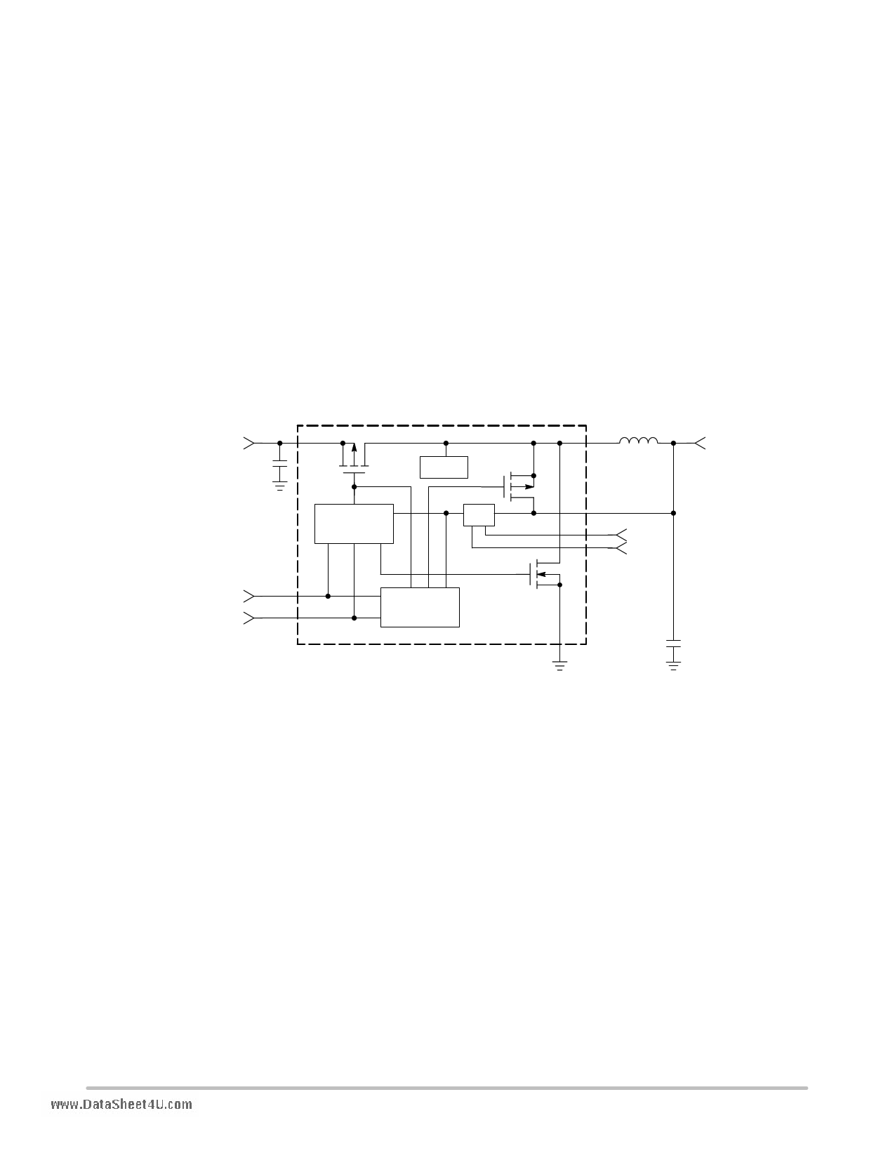
Vbat
Cin
10 m
Q1
DC/DC
CONTROL
Ilim Q3
EA
LX L1
10 mH
FB
CB0
CB1
Vout
Sync
SHD
LDO
CONTROL
Q2
Cout
10 m
Figure 3. Block Diagram and Circuit Schematic of the NCP1501
The external components required are an input and an
output 10 0 mF ceramic capacitor and a 10 mH inductor.
PWM Mode
During normal operation, a synchronization pulse acts as
the clock for the DC/DC controller. The rising edge of the
clock pulls the gate of Q1 low allowing the inductor to
charge. When the current through Q1 reaches either the
current limit or feedback voltage reaches its limit, Q1 will
turn off and Q2 will turn on. Q2 replaces the free wheeling
diode typically associated with Buck Converters. Q2 will
turn off when either a rising edge sync pulse is present or all
the stored energy is depleted from the inductor. Q3 remains
off during this mode.
The output voltage accuracy in the PWM mode is well
within 3% of the nominal set value. An over voltage
protection circuit is present in the PWM mode to limit the
positive voltage spike due to fast load transient conditions.
The PWM also has the ability to go to 100% duty cycle for
transient conditions and low input to output voltage
differentials.
In PWM mode, each switching cycle has a guaranteed
on−time of 100 ns. The NCP1501 has two protection circuits
that can eliminate the cycle. When tripped, the over voltage
protection or the thermal shutdown overrides the gate drive
of the high side MOSFET.
http://onsemi.com
5
5 Page 
2.0
1.8
1.6
1.4
1.2
1.0
0.8
0.6
0.4
0.2
0
0
NCP1501
1.80 Vout
1.57 Vout
1.35 Vout
1.05 Vout
1 23 45
Vin (V)
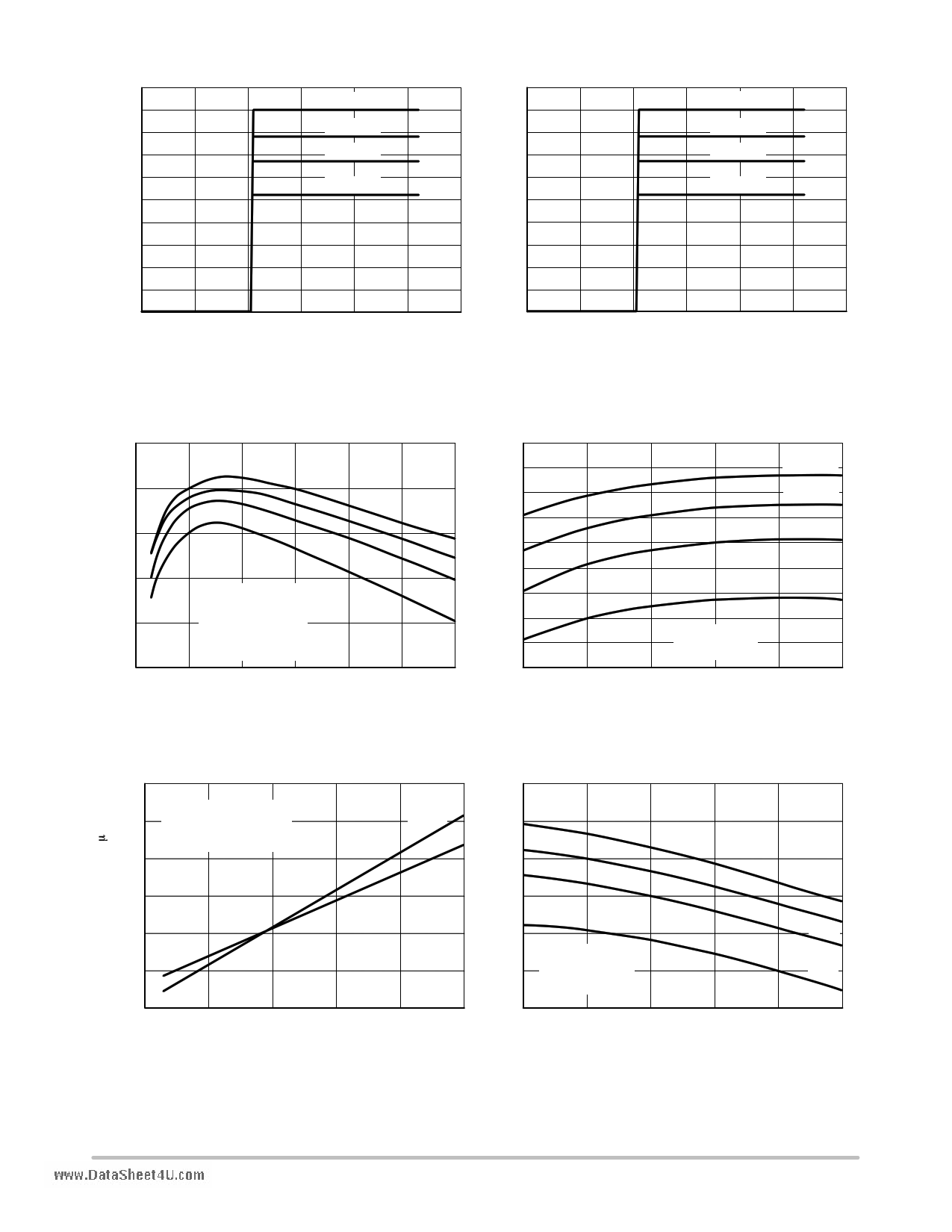
Figure 18. Output Voltage versus
PWM Input Voltage
2.0
1.8
1.6
1.4
1.2
1.0
0.8
0.6
0.4
0.2
0
60
1
1w.8w0 wVo.uDtataSheet4U.com
1.57 Vout
1.35 Vout
1.05 Vout
23 4
Vout (V)
5
6
Figure 19. Input Voltage versus Output Voltage
95
90
85
80
75
70
0
1.8 Vout
1.57
1.35
VCC = 3.6 V
Freq = 600 kHz
TA = 25°C
See Figure 9 for Circuit
1.05
50 100 150 200 250
Iout, OUTPUT CURRENT (mA)
300
Figure 20. Efficiency versus Output Current
92
91
90
89
88
87
86
85
84
83
500
1.80 Vout
1.57 Vout
1.35 Vout
1.05 Vout
Vin = 3.6 V
Iout = 100 mA
600 700 800
FREQUENCY (kHz)
900
1000
Figure 21. Efficiency versus Frequency
1200
1000
800
Vin = 3.6 V
Vout = 1.8 V
PWM Freq = 600 kHz
600
LDO
PWM
400
200
0
0 200 400 600 800 1000
Iout, OUTPUT CURRENT (mA)
Figure 22. Input Current versus Output Current
Comparison for PWM and LDO Mode
94
92
90
88
86
Iout = 100 mA
84 Freq = 600 kHz
TA = 25°C
82
2.7
3.2
3.7
4.2
Vin, INPUT VOLTAGE (V)
1.8 Vout
1.57
1.35
1.05
4.7 5.2
Figure 23. Efficiency versus Input Voltage
http://onsemi.com
11
11 Page | ||
| Páginas | Total 14 Páginas | |
| PDF Descargar | [ Datasheet NCP1501.PDF ] | |
Hoja de datos destacado
| Número de pieza | Descripción | Fabricantes |
| NCP1500 | Dual Mode PWM/Linear BUCK Converter | ON |
| NCP1500DMR2 | Dual Mode PWM/Linear BUCK Converter | ON |
| NCP1500DMR2G | Dual Mode PWM/Linear BUCK Converter | ON |
| NCP1501 | Dual Mode PWM/Linear Buck Converter | ON Semiconductor |
| Número de pieza | Descripción | Fabricantes |
| SLA6805M | High Voltage 3 phase Motor Driver IC. |
Sanken |
| SDC1742 | 12- and 14-Bit Hybrid Synchro / Resolver-to-Digital Converters. |
Analog Devices |
|
DataSheet.es es una pagina web que funciona como un repositorio de manuales o hoja de datos de muchos de los productos más populares, |
| DataSheet.es | 2020 | Privacy Policy | Contacto | Buscar |
