|
|
|
PDF NTMFS4852N Data sheet ( Hoja de datos )
| Número de pieza | NTMFS4852N | |
| Descripción | Power MOSFET ( Transistor ) | |
| Fabricantes | ON Semiconductor | |
| Logotipo | ||
Hay una vista previa y un enlace de descarga de NTMFS4852N (archivo pdf) en la parte inferior de esta página. Total 7 Páginas | ||
|
No Preview Available !
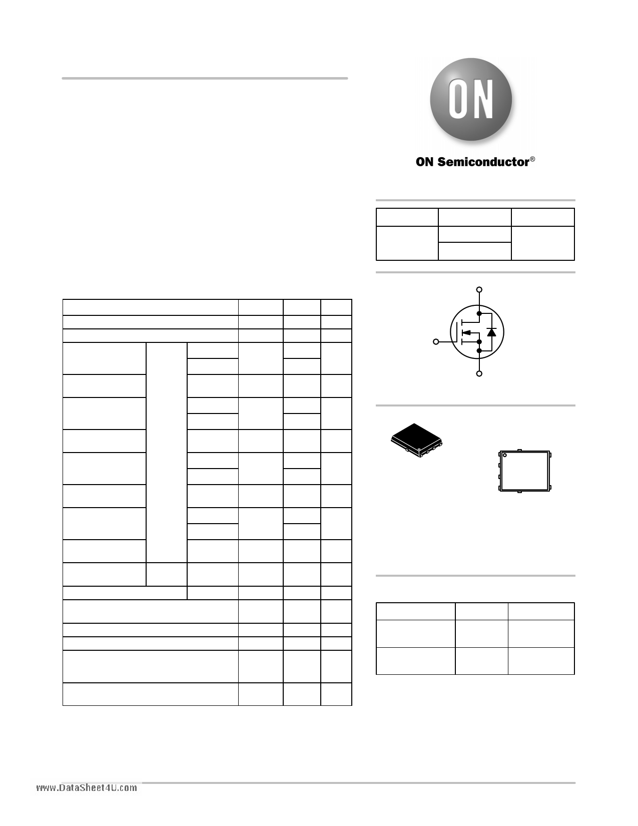
NTMFS4852N
Advance Information
Power MOSFET
30 V, 155 A, Single N−Channel, SO−8 FL
Features
• Low RDS(on) to Minimize Conduction Losses
• Low Capacitance to Minimize Driver Losses
• Optimized Gate Charge to Minimize Switching Losses
• These are Pb−Free Device
Applications
• Refer to Application Note AND8195/D
• CPU Power Delivery
• DC−DC Converters
• Low Side Switching
MAXIMUM RATINGS (TJ = 25°C unless otherwise stated)
Parameter
Symbol Value Unit
Drain−to−Source Voltage
Gate−to−Source Voltage
Continuous Drain
C(Nuortreen1t)RqJA
Power Dissipation
RqJA (Note 1)
Continuous Drain
Current
10 sec
RqJA
v
Power Dissipation
RqJA, t v 10 sec
Continuous Drain
C(Nuortreen2t)RqJA
Steady
State
Power Dissipation
RqJA (Note 2)
Continuous Drain
Current RqJC
(Note 1)
Power Dissipation
RqJC (Note 1)
Pulsed Drain
Current
tp=10ms
TA = 25°C
TA = 85°C
TA = 25°C
TA = 25°C
TA = 85°C
TA = 25°C
TA = 25°C
TA = 85°C
TA = 25°C
TC = 25°C
TC = 85°C
TC = 25°C
TA = 25°C
VDSS
VGS
ID
PD
ID
PD
ID
PD
ID
PD
IDM
30 V
±20 V
25 A
18
2.31 W
40 A
29
5.95 W
16 A
11
0.90 W
155 A
112
86.2 W
310 A
Current limited by package
TA = 25°C
Operating Junction and Storage
Temperature
Source Current (Body Diode)
Drain to Source dV/dt
Single Pulse Drain−to−Source Avalanche
Energy (VDD = 50 V, VGS = 10 V,
IL = 49 Apk, L = 0.3 mH, RG = 25 W)
Lead Temperature for Soldering Purposes
(1/8” from case for 10 s)
IDmaxpkg
TJ,
TSTG
IS
dV/dt
EAS
TL
100
−55 to
+150
72
6
360
260
A
°C
A
V/ns
mJ
°C
Stresses exceeding Maximum Ratings may damage the device. Maximum
Ratings are stress ratings only. Functional operation above the Recommended
Operating Conditions is not implied. Extended exposure to stresses above the
Recommended Operating Conditions may affect device reliability.
This document contains information on a new product. Specifications and information
herein are subject to change without notice.
© Semiconductor Components Industries, LLC, 2009
July, 2009 − Rev. P1
1
www.DataSheet4U.com
http://onsemi.com
V(BR)DSS
30 V
RDS(ON) MAX
2.1 mW @ 10 V
3.1 mW @ 4.5 V
ID MAX
155 A
D (5,6)
G (4)
S (1,2,3)
N−CHANNEL MOSFET
1
SO−8 FLAT LEAD
CASE 488AA
STYLE 1
MARKING
DIAGRAM
D
S
S
S
4852N
AYWWG
D
GGD
D
A = Assembly Location
Y = Year
WW = Work Week
G = Pb−Free Package
(Note: Microdot may be in either location)
ORDERING INFORMATION
Device
NTMFS4852NT1G
Package
SO−8FL
(Pb−Free)
Shipping†
1500 /
Tape & Reel
NTMFS4852NT3G SO−8FL
(Pb−Free)
5000 /
Tape & Reel
†For information on tape and reel specifications,
including part orientation and tape sizes, please
refer to our Tape and Reel Packaging Specifications
Brochure, BRD8011/D.
*For additional information on our Pb−Free strategy
and soldering details, please download the ON
Semiconductor Soldering and Mounting Techniques
Reference Manual, SOLDERRM/D.
Publication Order Number:
NTMFS4852N/D
1 page 
NTMFS4852N
TYPICAL CHARACTERISTICS
www.DataSheet4U.com
6000
5000
TJ = 25°C
Ciss VGS = 0 V
4000
3000
2000
Coss
1000 Crss
0
0 5 10 15 20 25 30
GATE−TO−SOURCE OR DRAIN−TO−SOURCE VOLTAGE (V)
Figure 7. Capacitance Variation
1000
100
VDD = 15 V
VGS = 10 V
ID = 15 A
10
td(off)
tf
tr
td(on)
1
1 10 100
RG, GATE RESISTANCE (W)
Figure 9. Resistive Switching Time Variation
vs. Gate Resistance
1000
100 10 ms
100 ms
10 1 ms
1 VGS = 30 V
Single Pulse
TC = 25°C
0.1 RDS(on) Limit
Thermal Limit
0.01 Package Limit
0.01 0.1
1
10 ms
dc
10 100
VDS, DRAIN−TO−SOURCE VOLTAGE (V)
Figure 11. Maximum Rated Forward Biased
Safe Operating Area
11
10 QT
9
8 VGS
7
6
5
4 Qgs
Qgd
3 VDD = 15 V
2
VGS = 10 V
ID = 30 A
1 TJ = 25°C
0
0 10 20 30 40 50 60 70 80
Qg, TOTAL GATE CHARGE (nC)
Figure 8. Gate−to−Source and
Drain−to−Source Voltage vs. Total Charge
30
VGS = 0 V
25 TJ = 25°C
20
15
10
5
0
0.4 0.5 0.6 0.7 0.8 0.9 1.0
VSD, SOURCE−TO−DRAIN VOLTAGE (V)
Figure 10. Diode Forward Voltage vs. Current
400
ID = 49 A
300
200
100
0
25 50 75 100 125 150
TJ, STARTING JUNCTION TEMPERATURE(°C)
Figure 12. Maximum Avalanche Energy vs.
Starting Junction Temperature
http://onsemi.com
5
5 Page | ||
| Páginas | Total 7 Páginas | |
| PDF Descargar | [ Datasheet NTMFS4852N.PDF ] | |
Hoja de datos destacado
| Número de pieza | Descripción | Fabricantes |
| NTMFS4852N | Power MOSFET ( Transistor ) | ON Semiconductor |
| NTMFS4852N | Power MOSFET ( Transistor ) | ON Semiconductor |
| Número de pieza | Descripción | Fabricantes |
| SLA6805M | High Voltage 3 phase Motor Driver IC. |
Sanken |
| SDC1742 | 12- and 14-Bit Hybrid Synchro / Resolver-to-Digital Converters. |
Analog Devices |
|
DataSheet.es es una pagina web que funciona como un repositorio de manuales o hoja de datos de muchos de los productos más populares, |
| DataSheet.es | 2020 | Privacy Policy | Contacto | Buscar |