|
|
|
PDF TB501-01 Data sheet ( Hoja de datos )
| Número de pieza | TB501-01 | |
| Descripción | Test Board for PLL501-01/-05 | |
| Fabricantes | PhaseLink Corporation | |
| Logotipo | ||
Hay una vista previa y un enlace de descarga de TB501-01 (archivo pdf) en la parte inferior de esta página. Total 1 Páginas | ||
|
No Preview Available !
T B 5 0 1 - 0 1 / - 0 5www.DataSheet4U.com
Test Board for PLL501-01/-05
This note documents the test board prepared for the PLL501-01 and PLL501-05
The test board is designed to simplify the testing of the PLL501-01 and PLL501-05, and implements the best approaches for
decoupling the VCXO chip using discrete external components.
While this test board achieves satisfactory decoupling results, best results are achieved when the VCXO chip is laid out into
the final PCB, following the recommendations indicated in the data sheet.
1. External Components and Layout Recommendations (as per PLL501-01/-05 data sheet)
The PLL501-01/-05 requires a minimum number of external components for proper operation. A standard low frequency
decoupling capacitor of 4.7µF or more should be used between VDD and GND (pin 2 and pin 4, as well as pin 6 and pin 7).
Additionally, higher frequency decoupling capacitors of 0.1µF are required between VDD and GND (between pin 2 and 4,
and between pin 6 and 7). These higher frequency decoupling capacitors must be connected as close to the PLL501-01/-05
chip as possible, and preferably directly next to the PLL501-01/-05 pins. A series termination resistor of 33Ω may be used
for the clock output (series termination resistor not implemented on test board).
The input crystal must be connected as close to the chip as possible, and preferably directly next to the PLL501-01/-05
pins. If a crystal with CL higher than 10pF is used, it will requires additional loading capacitors externally to
complement the internal 10pF of the PLL501-01/-05: one between each crystal electrode and GND, as close to the
crystal as possible, and preferably directly next to the crystal electrodes. Consult PhaseLink for recommended suppliers.
2. Crystal Specifications (as per PLL501-01/-05 data sheet)
PARAMETERS
Crystal Resonator Frequency
Crystal Loading Capacitance Rating
Crystal Pullability
Recommended ESR
SYMBOL
FXIN
CL (xtal)
C0/C1 (xtal)
RE
CONDITIONS
Parallel Fundamental Mode
AT cut
AT cut
MIN. TYP. MAX. UNITS
10 20 MHz
10 pF
250 -
30 Ω
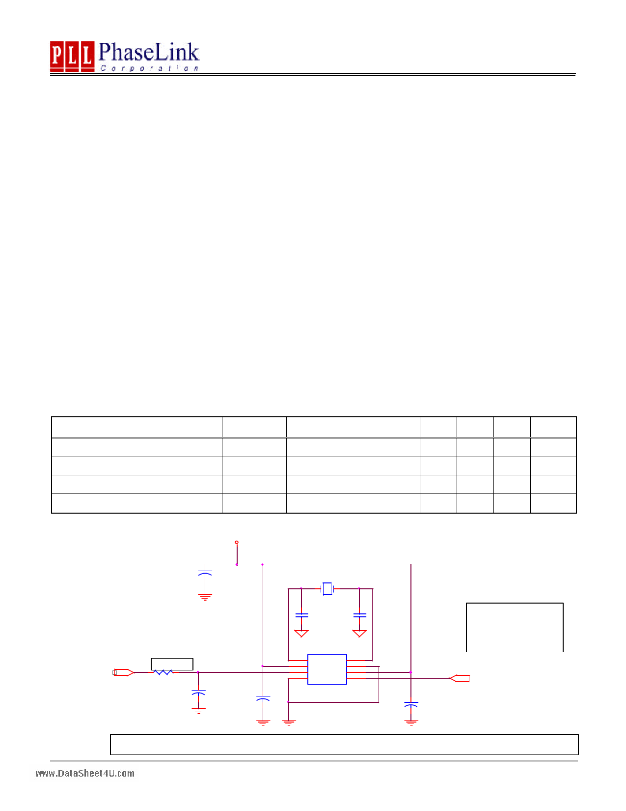
3. Test board schematic
+3.3V
C3
4.7 uf
XTAL, NSK 17.664 MHz, 14 pF
17.664 MHz
Y1
Vin control
R1 = 0Ω
?
R1= 0 or 10
C6
0.1uf
C1
0.1uf
C5 C4
10 pF 10 pF
U1
1
2
3
4
XIN XOUT
VDD GND
CTRL VDD
GND CLK
PLL501-01
8
7
6
5
Note: C5 and C4 are only
required if a crystal
of CL greater than
10 pF is used.
Clock output
C2
0.1uf
Please order a test board without external C5 and C4 capacitors if you intend to use a crystal of CL equal to 10pF.
47745 Fremont Blvd., Fremont, California 94538 TEL (510) 492-0990 FAX (510) 492-0991
Rev 5/10/01 Page 1
1 page | ||
| Páginas | Total 1 Páginas | |
| PDF Descargar | [ Datasheet TB501-01.PDF ] | |
Hoja de datos destacado
| Número de pieza | Descripción | Fabricantes |
| TB501-01 | Test Board for PLL501-01/-05 | PhaseLink Corporation |
| TB501-05 | Test Board for PLL501-01/-05 | PhaseLink Corporation |
| Número de pieza | Descripción | Fabricantes |
| SLA6805M | High Voltage 3 phase Motor Driver IC. |
Sanken |
| SDC1742 | 12- and 14-Bit Hybrid Synchro / Resolver-to-Digital Converters. |
Analog Devices |
|
DataSheet.es es una pagina web que funciona como un repositorio de manuales o hoja de datos de muchos de los productos más populares, |
| DataSheet.es | 2020 | Privacy Policy | Contacto | Buscar |