|
|
PDF LX128B Data sheet ( Hoja de datos )
| Número de pieza | LX128B | |
| Descripción | High Performance Interfacing and Switching | |
| Fabricantes | Lattice Semiconductor | |
| Logotipo | ||
Hay una vista previa y un enlace de descarga de LX128B (archivo pdf) en la parte inferior de esta página. Total 70 Páginas | ||
|
No Preview Available !
www.DataSheet4U.com
ispGDX2™ Family
Includes
High-
High Performance Interfacing and Switching
September 2005
Features
Performance,
Low-Cost
“E-Series” ■ Two Options Available
Data Sheet
• High-performance sysHSI (standard part number)
■ High Performance Bus Switching
• Low-cost, no sysHSI (“E-Series”)
• High bandwidth
– Up to 12.8 Gbps (SERDES)
■ sysHSI Blocks Provide up to 16 High-speed
– Up to 38 Gbps (without SERDES)
Channels
• Up to 16 (15x10) FIFOs for data buffering
• Serializer/de-serializer (SERDES) included
• High speed performance
• Clock Data Recovery (CDR) built in
– fMAX = 360MHz
– tPD = 3.0ns
– tCO = 2.9ns
– tS = 2.0ns
• Built-in programmable control logic capability
• 800 Mbps per channel
• LVDS differential support
• 10B/12B support
– Encoding / decoding
– Bit alignment
• I/O intensive: 64 to 256 I/Os
– Symbol alignment
• Expanded MUX capability up to 188:1 MUX
• 8B/10B support
– Bit alignment
■ sysCLOCK™ PLL
– Symbol alignment
• Frequency synthesis and skew management
• Source Synchronous support
• Clock multiply and divide capability
• Clock shifting up to +/-2.35ns in 335ps steps
■ Flexible Programming and Testing
• Up to four PLLs
• IEEE 1532 compliant In-System Programmabil-
ity (ISP™)
■ sysIO™ Interfacing
• Boundary scan test through IEEE 1149.1
• LVCMOS 1.8, 2.5, 3.3 and LVTTL support for
interface
standard board interfaces
• 3.3V, 2.5V or 1.8V power supplies
• SSTL 2/3 Class I and II support
• 5V tolerant I/O for LVCMOS 3.3 and LVTTL
• HSTL Class I, III and IV support
interfaces
• GTL+, PCI-X for bus interfaces
• LVPECL, LVDS and Bus LVDS differential support
• Hot socketing
• Programmable drive strength
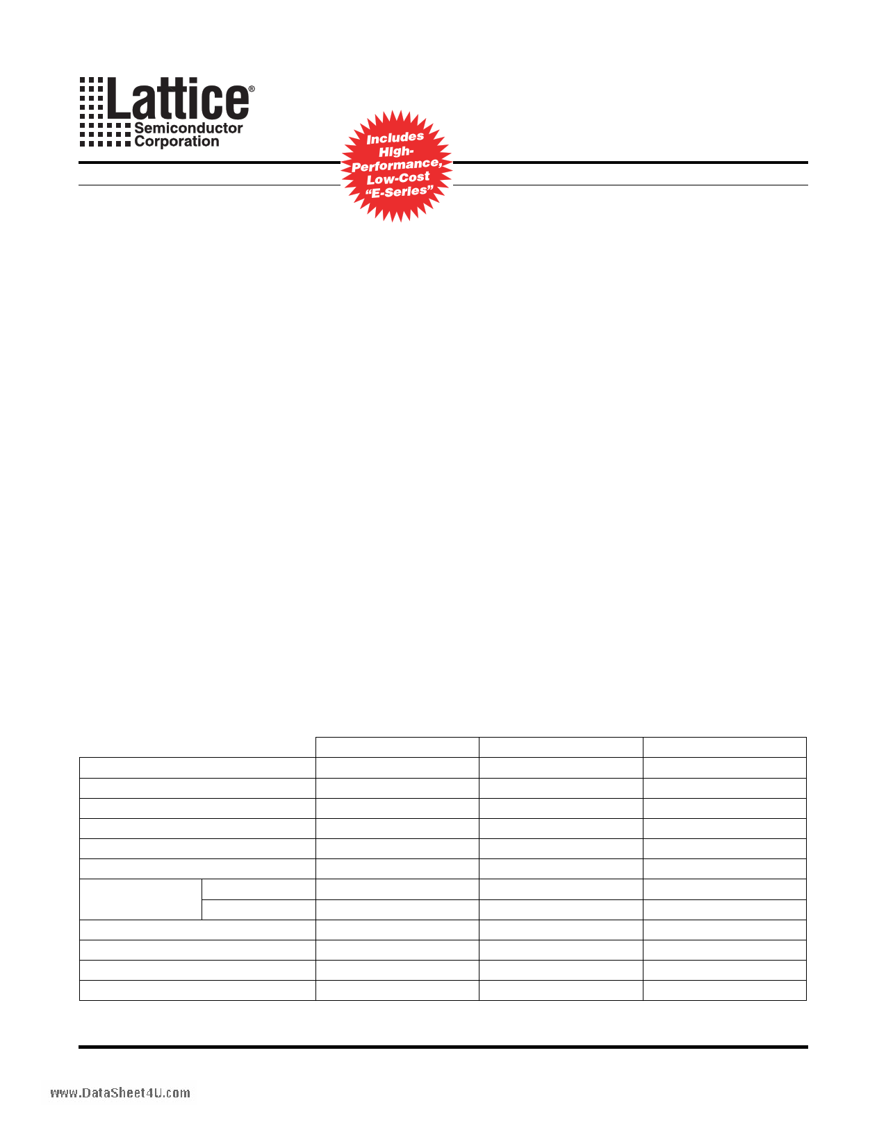
Table 1. ispGDX2 Family Selection Guide
ispGDX2-64/E
ispGDX2-128/E
ispGDX2-256/E
I/Os 64 128 256
GDX Blocks
4 8 16
tPD
tS
tCO
fMAX (Toggle)
Max Bandwidth
sysHSI Channels2
SERDES1, 2
Without SERDES3
3.0ns
2.0ns
2.9ns
360MHz
3.2Gbps
11Gbps
4
3.2ns
2.0ns
3.1ns
330MHz
6.4Gbps
21Gbps
8
3.5ns
2.0ns
3.2ns
300MHz
12.8Gbps
38Gbps
16
LVDS/Bus LVDS (Pairs)
32 64 128
PLLs
224
Package
100-ball fpBGA
208-ball fpBGA
484-ball fpBGA
1. Max number of SERDES channels per device * 800Mbps
2. “E-Series” does not support sysHSI.
3. fMAX (Toggle) * maximum I/Os divided by 2.
© 2005 Lattice Semiconductor Corp. All Lattice trademarks, registered trademarks, patents, and disclaimers are as listed at www.latticesemi.com/legal. All other brand
or product names are trademarks or registered trademarks of their respective holders. The specifications and information herein are subject to change without notice.
www.latticesemi.com
1
gdx2fam_13
1 page 
Lattice Semiconductor
Figure 2. GDX Block
GRP
GDX Block
32 bits
MUX
Control Select
Control Array
4 bits
8
8
8
2
Nibble 0
MUX and Register
Block (MRB)
0
ispGDX2 Fwawmwi.lDyatDaSahteaetS4Uh.ceoemt
sysIO Bank
OE
IN
OUT
4 bits
4 bits
8
2 MUX and Register
Block (MRB)
1
8
2 MUX and Register
Block (MRB)
2
OE
IN
OUT
OE
IN
OUT
4 bits
8
2 MUX and Register
Block (MRB)
3
OE
IN
OUT
16 bits
4
16 bits
4
16 bits
4
8
2
8
2
8
2
Nibble 1
MRBs 4-7
Nibble 2
MRBs 8-11
Nibble 3
MRBs 12-15
OE
IN
OUT
OE
IN
OUT
OE
IN
OUT
The output register of the MRB has a built-in bi-directional shift register capability. Each output register correspond-
ing to MRB “n”, receives data output from its two adjacent MRBs, MRB (n-1) and MRB (n+1), to provide shift regis-
ter capability. Like the output register, each input register of the MRB has built-in shift register capability. Each input
register can receive data from its two adjacent MRB input registers, to provide bi-directional shift register capability.
The chaining crosses GDX Block boundaries. The chain of input registers and the chain of output registers can be
combined as one shift register via the GRP.
5
5 Page 
Lattice Semiconductor
Figure 7. I/O Pin Connection to the sysCLOCK PLL1
PLL_LOCK
CLK_OUT
GCLK_IN
Input Clock
(M) Divider
÷ 1 to 32
Programmable
+ Delay
--------------------
Programmable
- Delay
PLL (n)
Post-scalar
(V) Divider
÷
1, 2, 4, 8,
16, 32
Clock
(K) Divider
÷
2, 4, 8,
16, 32
Feedback
Divider (N)
x 1 to 32
Clock Net
To Adjacent_PLL
From Adjacent_PLL
PLL_FBK
GRP
PLL_RST
ispGDX2 Fwawmwi.lDyatDaSahteaetS4Uh.ceoemt
Output
Reg/
Latch
Input
Reg/
Latch
Delay
GDX Block
GCLK_IN
1. Some pins are shared. See Logic Signal Connections Table for details.
Resetb (0)
Control Array
(from selected blocks)
11
11 Page | ||
| Páginas | Total 70 Páginas | |
| PDF Descargar | [ Datasheet LX128B.PDF ] | |
Hoja de datos destacado
| Número de pieza | Descripción | Fabricantes |
| LX128B | High Performance Interfacing and Switching | Lattice Semiconductor |
| LX128B-32F208C | High Performance Interfacing and Switching | Lattice Semiconductor |
| LX128B-5F208C | High Performance Interfacing and Switching | Lattice Semiconductor |
| LX128C | High Performance Interfacing and Switching | Lattice Semiconductor |
| Número de pieza | Descripción | Fabricantes |
| SLA6805M | High Voltage 3 phase Motor Driver IC. |
Sanken |
| SDC1742 | 12- and 14-Bit Hybrid Synchro / Resolver-to-Digital Converters. |
Analog Devices |
|
DataSheet.es es una pagina web que funciona como un repositorio de manuales o hoja de datos de muchos de los productos más populares, |
| DataSheet.es | 2020 | Privacy Policy | Contacto | Buscar |
