|
|
PDF MAX1213 Data sheet ( Hoja de datos )
| Número de pieza | MAX1213 | |
| Descripción | 250Msps Analog-to-Digital Converter | |
| Fabricantes | Maxim Integrated Products | |
| Logotipo |  |
|
Hay una vista previa y un enlace de descarga de MAX1213 (archivo pdf) en la parte inferior de esta página. Total 20 Páginas | ||
|
No Preview Available !
19-1003; Rev 2; 6/05
EVAALVUAAILTAIOBNLEKIT
www.DataSheet4U.com
1.8V, 12-Bit, 170Msps ADC for
Broadband Applications
General Description
The MAX1213 is a monolithic, 12-bit, 170Msps analog-
to-digital converter (ADC) optimized for outstanding
dynamic performance at high-IF frequencies up to
300MHz. The product operates with conversion rates
up to 170Msps while consuming only 788mW.
At 170Msps and an input frequency up to 250MHz, the
MAX1213 achieves a spurious-free dynamic range
(SFDR) of 72.9dBc. Its excellent signal-to-noise ratio
(SNR) of 65.8dB at 10MHz remains flat (within 2dB) for
input tones up to 250MHz. This ADC yields an excellent
low-noise floor of -68dBFS, which makes it ideal for
wideband applications such as cable head-end
receivers and power-amplifier predistortion in cellular
base-station transceivers.
The MAX1213 requires a single 1.8V supply. The analog
input is designed for either differential or single-ended
operation and can be AC- or DC-coupled. The ADC also
features a selectable on-chip divide-by-2 clock circuit,
which allows the user to apply clock frequencies as high
as 340MHz. This helps to reduce the phase noise of the
input clock source. A low-voltage differential signal
(LVDS) sampling clock is recommended for best perfor-
mance. The converter’s digital outputs are LVDS com-
patible and the data format can be selected to be either
two’s complement or offset binary.
The MAX1213 is available in a 68-pin QFN package
with exposed paddle (EP) and is specified over the
industrial (-40°C to +85°C) temperature range.
See the Pin-Compatible Versions table for a complete
selection of 8-bit, 10-bit, and 12-bit high-speed ADCs in
this family.
Applications
Base-Station Power-Amplifier Linearization
Cable Head-End Receivers
Wireless and Wired Broadband Communication
Communications Test Equipment
Radar and Satellite Subsystems
Features
o 170Msps Conversion Rate
o Low Noise Floor of -68dBFS
o Excellent Low-Noise Characteristics
SNR = 65.8dB at fIN = 65MHz
SNR = 64.5dB at fIN = 250MHz
o Excellent Dynamic Range
SFDR = 76.5dBc at fIN = 65MHz
SFDR = 72.9dBc at fIN = 250MHz
o 59.5dB NPR for fNOTCH = 28.8MHz and a Noise
Bandwidth of 50MHz
o Single 1.8V Supply
o 788mW Power Dissipation at fSAMPLE = 170MHz
and fIN = 65MHz
o On-Chip Track-and-Hold Amplifier
o Internal 1.23V-Bandgap Reference
o On-Chip Selectable Divide-by-2 Clock Input
o LVDS Digital Outputs with Data Clock Output
o MAX1213 EV Kit Available
Ordering Information
PART
TEMP RANGE
MAX1213EGK -40°C to +85°C
*EP = Exposed paddle.
PIN-PACKAGE
68 QFN-EP*
PART
MAX1121
MAX1122
MAX1123
MAX1124
MAX1213
MAX1214
MAX1215
Pin-Compatible Versions
RESOLUTION
(BITS)
8
10
10
10
12
12
12
SPEED GRADE
(Msps)
250
170
210
250
170
210
250
Pin Configuration appears at end of data sheet.
________________________________________________________________ Maxim Integrated Products 1
For pricing, delivery, and ordering information, please contact Maxim/Dallas Direct! at
1-888-629-4642, or visit Maxim’s website at www.maxim-ic.com.
1 page 
www.DataSheet4U.com
1.8V, 12-Bit, 170Msps ADC for
Broadband Applications
Typical Operating Characteristics
(AVCC = OVCC = 1.8V, AGND = OGND = 0, fSAMPLE = 170MHz, AIN = -1dBFS; see each TOC for detailed information on test condi-
tions, differential input drive, differential sine-wave clock input drive, 0.1µF capacitor on REFIO, internal reference, digital output pins
differential RL = 100Ω, TA = +25°C.)
FFT PLOT
(8192-POINT DATA RECORD)
0
-10
fSAMPLE = 170MHz
fIN = 12.47192MHz
-20 AIN = -1.001dBFS
-30
SNR = 66.7dB
SINAD = 66.4dB
-40 SFDR = 83.8dBc
-50 HD2 = -83.8dBc
HD3 = -84dBc
-60
-70 HD2 HD3
-80
-90
FFT PLOT
(8192-POINT DATA RECORD)
0
-10
fSAMPLE = 170MHz
fIN = 65.09888MHz
-20 AIN = -1.099dBFS
-30 SNR = 66.5dB
SINAD = 65.7dB
-40 SFDR = 76dBc
-50 HD2 = -77.7dBc
HD3 = -76dBc
-60
-70
HD3 HD2
-80
-90
FFT PLOT
(8192-POINT DATA RECORD)
0
-10
fSAMPLE = 170MHz
fIN = 200.11108MHz
-20 AIN = -1.025dBFS
-30
SNR = 65dB
SINAD = 63.9dB
-40 SFDR = 70.7dBc
-50 HD2 = -74.8dBc
HD3 = -70.7dBc
-60
HD2 HD3
-70
-80
-90
-100
-110
0
10 20 30 40 50 60 70 80
ANALOG INPUT FREQUENCY (MHz)
-100
-110
0
10 20 30 40 50 60 70 80
ANALOG INPUT FREQUENCY (MHz)
-100
-110
0
10 20 30 40 50 60 70 80
ANALOG INPUT FREQUENCY (MHz)
FFT PLOT
(8192-POINT DATA RECORD)
0
fSAMPLE = 170MHz
-10 fIN = 250.04038MHz
-20 AIN = -1.040dBFS
-30
SNR = 64.5dB
SINAD = 63.5dB
-40 SFDR = 72.9dBc
-50 HD2 = -77.4dBc
HD3 = -72.9dBc
-60
-70 HD2
HD3
-80
-90
-100
-110
0 10 20 30 40 50 60 70 80
ANALOG INPUT FREQUENCY (MHz)
TWO-TONE IMD PLOT
(8192-POINT DATA RECORD)
0
-10
fSAMPLE = 170MHz
fIN1 = 99.25659MHz
-20 fIN2 = 101.08276MHz
-30 AIN1 = AIN2 = -6.974dBFS
IMD = -78dBc
-40
fIN2
fIN1
-50
-60
-70 fIN1 - fIN2 fIN1 + fIN2 3fIN2 - 2fIN1
-80
2fIN1
- fIN2
-90
-100
-110
0 10 20 30 40 50 60 70 80
ANALOG INPUT FREQUENCY (MHz)
SNR/SINAD vs. ANALOG INPUT FREQUENCY
(fSAMPLE = 170MHz, AIN = -1dBFS)
70
SNR
65
SINAD
60
55
50
45
0
50 100 150 200 250 300
fIN (MHz)
SFDR vs. ANALOG INPUT FREQUENCY
(fSAMPLE = 170MHz, AIN = -1dBFS
95
90
85
80
75
70
65
60
55
50
45
40
0
50 100 150 200 250 300
fIN (MHz)
HD2/HD3 vs. ANALOG INPUT FREQUENCY
(fSAMPLE = 170MHz, AIN = -1dBFS)
-50
-55
-60
-65 HD3
-70
-75
-80
-85 HD2
-90
-95
-100
0
50 100 150 200 250 300
fIN (MHz)
SNR/SINAD vs. ANALOG INPUT AMPLITUDE
(fSAMPLE = 170MHz, fIN = 65.098877MHz)
70
SNR
60
50
SINAD
40
30
20
10
-55 -50 -45 -40 -35 -30 -25 -20 -15 -10 -5 0
ANALOG INPUT AMPLITUDE (dBFS)
_______________________________________________________________________________________ 5
5 Page 
www.DataSheet4U.com
1.8V, 12-Bit, 170Msps ADC for
Broadband Applications
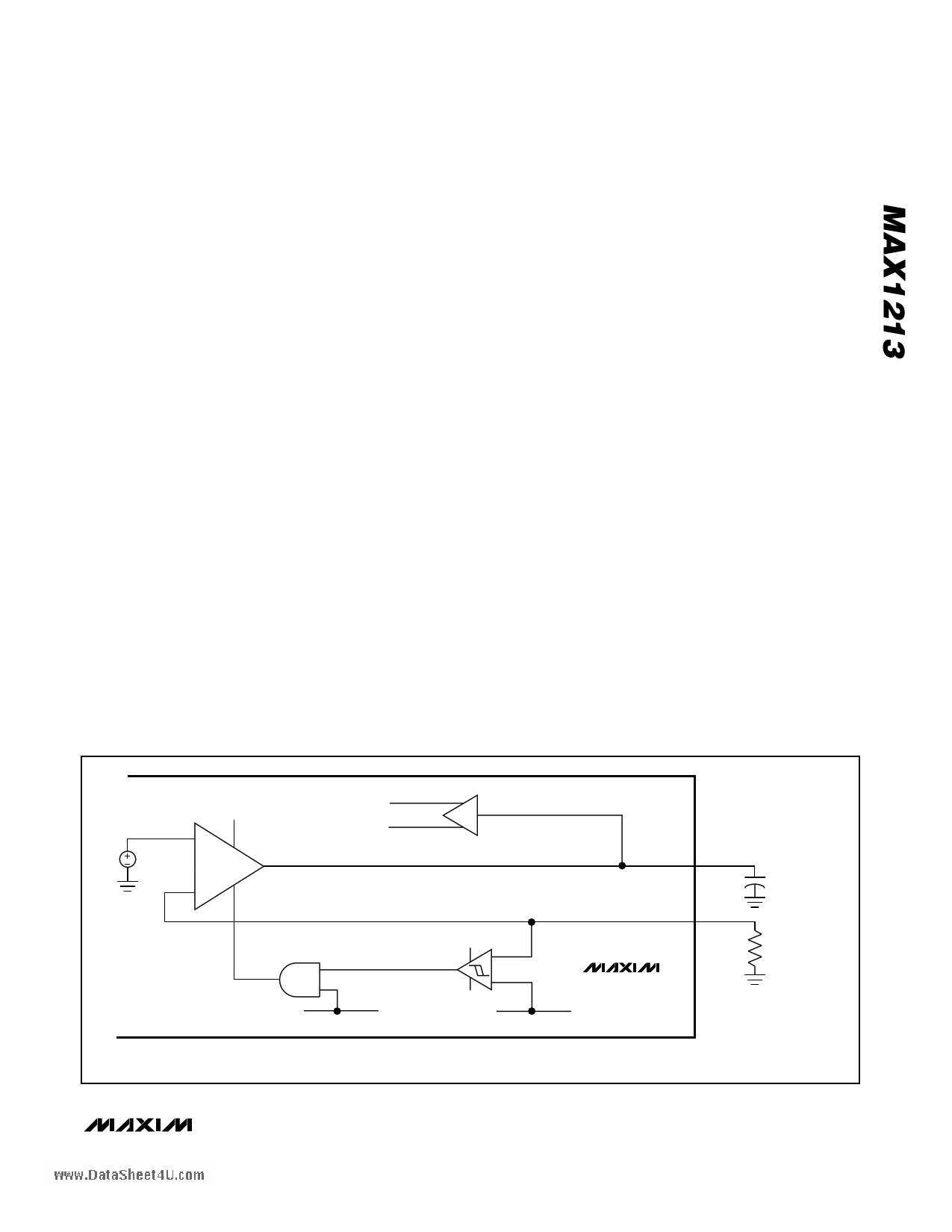
On-Chip Reference Circuit
The MAX1213 features an internal 1.23V bandgap refer-
ence circuit (Figure 3), which in combination with an inter-
nal reference-scaling amplifier determines the FSR of the
MAX1213. Bypass REFIO with a 0.1µF capacitor to
AGND. To compensate for gain errors or increase the
ADC’s FSR, the voltage of this bandgap reference can be
indirectly adjusted by adding an external resistor (e.g.,
100kΩ trim potentiometer) between REFADJ and AGND
or REFADJ and REFIO. See the Applications Information
section for a detailed description of this process.
To disable the internal reference, connect REFADJ to
AVCC. In this configuration, an external, stable refer-
ence must be applied to REFIO to set the converter’s
full scale. To enable the internal reference, connect
REFADJ to AGND.
Clock Inputs (CLKP, CLKN)
Designed for a differential LVDS clock input drive, it is
recommended to drive the clock inputs of the MAX1213
with an LVDS- or LVPECL-compatible clock to achieve
the best dynamic performance. The clock signal source
must be a high-quality, low-phase noise with fast edge
rates to avoid any degradation in the noise performance
of the ADC. The clock inputs (CLKP, CLKN) are internal-
ly biased to 1.15V, accept a typical differential signal
swing of 0.5VP-P, and are usually driven in AC-coupled
configuration. See the Differential, AC-Coupled PECL-
Compatible Clock Input section for more circuit details
on how to drive CLKP and CLKN appropriately. Although
not recommended, the clock inputs also accept a single-
ended input signal.
The MAX1213 also features an internal clock-manage-
ment circuit (duty-cycle equalizer) that ensures that the
clock signal applied to inputs CLKP and CLKN is
processed to provide a 50% duty-cycle clock signal
that desensitizes the performance of the converter to
variations in the duty cycle of the input clock source.
Note that the clock duty-cycle equalizer cannot be
turned off externally and requires a minimum clock fre-
quency of >20MHz to work appropriately and accord-
ing to data sheet specifications.
Data Clock Outputs (DCLKP, DCLKN)
The MAX1213 features a differential clock output, which
can be used to latch the digital output data with an
external latch or receiver. Additionally, the clock output
can be used to synchronize external devices (e.g.,
FPGAs) to the ADC. DCLKP and DCLKN are differential
outputs with LVDS-compatible voltage levels. There is a
4.95ns delay time between the rising (falling) edge of
CLKP (CLKN) and the rising edge of DCLKP (DCLKN).
See Figure 4 for timing details.
Divide-by-2 Clock Control (CLKDIV)
The MAX1213 offers a clock control line (CLKDIV),
which supports the reduction of clock jitter in a system.
Connect CLKDIV to OGND to enable the ADC’s internal
divide-by-2 clock divider. Data is now updated at one-
half the ADC’s input clock rate. CLKDIV has an internal
pulldown resistor and can be left open for applications
that require this divide-by-2 mode. Connecting CLKDIV
to OVCC disables the divide-by-2 mode.
ADC FULL SCALE = REFT-REFB
REFERENCE
1V BUFFER
REFT REFERENCE
SCALING AMPLIFIER
G
REFB
REFIO
0.1µF
CONTROL LINE TO
DISABLE REFERENCE BUFFER
REFADJ
100Ω*
AVCC
REFT: TOP OF REFERENCE LADDER.
REFB: BOTTOM OF REFERENCE LADDER.
Figure 3. Simplified Reference Architecture
AVCC/2
MAX1213
*REFADJ MAY
BE SHORTED TO
AGND DIRECTLY
______________________________________________________________________________________ 11
11 Page | ||
| Páginas | Total 20 Páginas | |
| PDF Descargar | [ Datasheet MAX1213.PDF ] | |
Hoja de datos destacado
| Número de pieza | Descripción | Fabricantes |
| MAX121 | 308Ksps ADC with DSP Interface and 78dB SINAD | Maxim Integrated |
| MAX1211 | IF Sampling ADC | Maxim Integrated |
| MAX1213 | 170Msps ADC | Maxim Integrated |
| MAX1213 | 250Msps Analog-to-Digital Converter | Maxim Integrated Products |
| Número de pieza | Descripción | Fabricantes |
| SLA6805M | High Voltage 3 phase Motor Driver IC. |
Sanken |
| SDC1742 | 12- and 14-Bit Hybrid Synchro / Resolver-to-Digital Converters. |
Analog Devices |
|
DataSheet.es es una pagina web que funciona como un repositorio de manuales o hoja de datos de muchos de los productos más populares, |
| DataSheet.es | 2020 | Privacy Policy | Contacto | Buscar |
