|
|
|
PDF LX1734 Data sheet ( Hoja de datos )
| Número de pieza | LX1734 | |
| Descripción | 1.0MHz Inverting DC/DC Converter | |
| Fabricantes | Microsemi Corporation | |
| Logotipo | ||
Hay una vista previa y un enlace de descarga de LX1734 (archivo pdf) en la parte inferior de esta página. Total 8 Páginas | ||
|
No Preview Available !
LX1734
www.DataSheet4U.com
TM ® 1.0MHz Inverting DC/DC Converter
DESCRIPTION
The LX1734 is an inverting Fixed frequency operation ensures a
DC/DC current-mode controller. With clean output free from low frequency
a 750mA integrated switch, the noise typically present with charge pump
LX1734 can generate large output solutions. The low impedance output
currents in a small footprint. The remains within 1% of nominal during
LX1734 minimizes external com- large load steps. The 18V switch allows
ponent size and cost by implementing high voltage outputs to be generated.
a high switching frequency of The LX1734 is available in the space
1.0MHz, while generating -5V at saving 6-lead 3x3 Jedec MO-229
250mA.
package, which has the same footprint
When configured in the dual and lead spacing as the SOT-23A. A
inductor inverting topology very low complete inverter function utilizes less
output voltage ripple approaching than 0.32 inches of PCB space.
1mVP-P can be achieved when used in
conjunction with ceramic output
capacitors. The dual inductor can be
implemented as a coupled or separate
cores.
IMPORTANT: For the most current data, consult MICROSEMI’s website: http://www.microsemi.com
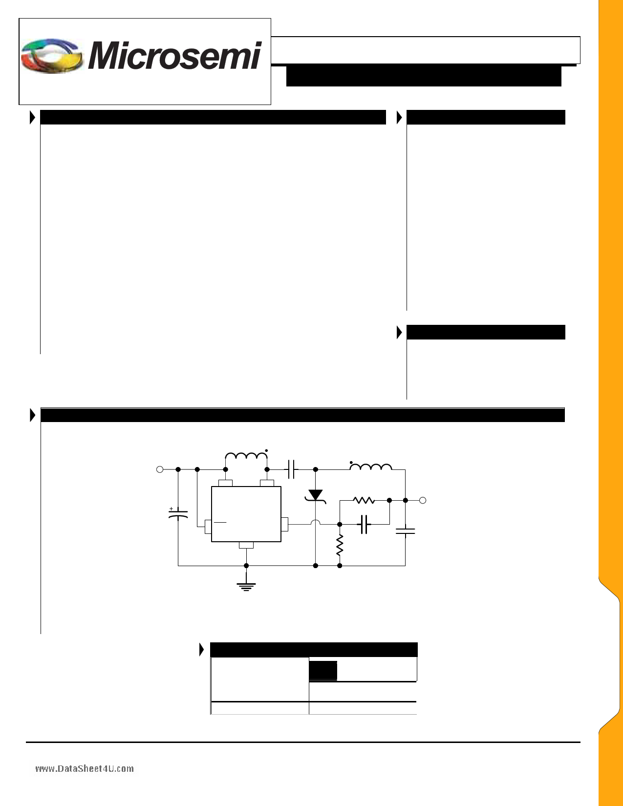
VIN = 5V
C1
10µF
PRODUCT HIGHLIGHT
L1A
22µH
C2
1µF
L1B
22µH
VIN SW
LX1734
SD NFB
GND
R1
29.4k
R2
10k C4
1000pF
KEY FEATURES
Fixed Frequency 1.0MHz
Operation
Very Low Noise: 1mVP-P Output
Ripple Possible With Cuk
Topology
Stable Operation With Ceramic or
Tantalum Capacitors
-5V at 250mA from 5V Input
Uses Small Surface Mount L/C
Components
Wide Input Range: 4.2V to 8V
Low VCESAT Switch: 600mV at
600mA
6-Lead 3x3mm JEDEC MLPM
Package
Functionally Compatible with
LT1611 or LT1931
APPLICATIONS/BENEFITS
Disk Drive MR Head Bias
Digital Camera CCD Bias
LCD Bias
GaAs FET Bias
Local -5V or -12V Supplies
VOUT = -5V
@ 150mA
C3
22µF
Note: L1A and L1B are shown as coupled. Individual inductors can also be used.
C1, C2, C3 are ceramic capacitors
Figure 1
Copyright © 2002
Rev. 3.0a, 2005-03-14
PACKAGE ORDER INFO
TA (°C)
Plastic MLPL
LM 6-Pin
RoHS Compliant / Pb-free
Transition DC: 0452
0 to 85
LX1734CLM
Note: Available in Tape & Reel. Append the letters “TR” to the
part number. (i.e. LX1734CLM-TR)
Microsemi
Microsemi Integrated Products
11861 Western Avenue, Garden Grove, CA. 92841, 714-898-8121, Fax: 714-893-2570
Page 1
1 page 
LX1734
www.DataSheet4U.com
TM ® 1.0MHz Inverting DC/DC Converter
THEORY OF OPERATION
The LX1734 is a fixed frequency current mode controller
designed to develop a negative output voltage from a positive
input voltage. The switching transistor and current sense resistor
are integrated into the part. The PWM functions in a peak current
regulation mode using the amplified error signal to determine the
peak switch current each cycle. Slope compensation is added to
provide stable operation at high duty cycles. A current limit
detector overrides the regulation loop and prevents the switch
current from exceeding the over current threshold level.
The bandgap control circuit keeps Q1 biased on and produces a
reference current (IREF) that produces a voltage drop across the
internal resistance that has a positive temperature coefficient.
When this resistor voltage drop is added to the negative temperature
coefficient of the base-emitter voltage drop of Q1, the result is a
temperature compensated reference voltage (VREF) at the NFB pin.
The summing node from the external feedback network is
connected directly to NFB pin, which is relatively high impedance
(typically 150k). The feedback loop minimizes the error current,
(IERROR) which effectively regulates the voltage at the NFB pin. As
with a conventional error amplifier, the error signal is proportional
to the difference between the temperature compensated reference
voltage (VREF) and the summing node voltage. A slight correction
factor is necessary to account for the added summing node voltage
due to the reference current (IREF, typically 4µADC) flowing
through the Thevenin equivalent summing node external resistance.
APPLICATION NOTE
The LX1734 can be used in several topologies that generate a
negative output voltage from a positive input voltage. The
LX1734 can be used in a dual inductor converter with coupled or
uncoupled inductors (see Figure 1); this topology is required if
the absolute value of the output voltage is less than or equal to
the input voltage but can also be used for higher voltage outputs.
The following components or their equivalents can be used to
implement the converter in Figure 1, which produces a –5V
output at 150mA from a +5V input. The reference design has an
efficiency of greater than 72% and an input ripple voltage of less
than 6mVP-P and an output ripple voltage of less than 300µVP-P.
Ref Description
Part Number
Manufacturer
C1 Ceramic, 4.7uF,
JMK212BJ475MG
Taiyo Yuden
6.3V (0805)
C2 Ceramic, 1uF, 16V GRM40X7R105M16
Murata
(0805)
C3 Ceramic, 22uF,
JMK325BJ226MM
Taiyo Yuden
6.3V (1210)
C4 Ceramic, 470pF, GRM36X7R471K050
Murata
50V (0402)
D1 Diode, 0.5A, 30V
UPS530
Microsemi
L1 Inductor, Coupled,
CLS62-220NC
Sumida
22uH
Table 1 - Part List for Figure 1 (All Parts Are Surface Mount).
Separate inductors (not on a common core) can be used in place
of the coupled inductor (L1) of Figure 1. In this case the only
component that changes in the parts list is L1, which now would
be two separate inductors (L1, formerly L1A, and L2, formerly
L1B). With the separate inductors the peak-to-peak voltage
ripple on the input the output were less the 2mVP-P and less than
500µVP-P, respectively.
Table 2 - Part List For Alternative Inductors
Ref.
Designator
L1, L2
Description
Inductor, 47uH,
(1812)
Part Number
Manufacturer
LQH4C470K04M00
Murata
Inductor Selection
When the LX1734 is used in a dual inductor converter with coupled
inductors, a parallel winding inductor value of 22µH works well for
a 5V input and a -5V output at 150mA. The inductor value can be
scaled to the particular set of operating conditions based on the
input voltage, output voltage, and output current. The new value of
coupled inductor parallel inductance can be calculated using the
following equation:
L NEW
=
22µH× ⎜⎛
⎝
VIN
5V
⎟⎞
⎠
×
⎜⎜⎝⎛
150 mA
IOUT
⎟⎟⎠⎞× ⎜⎜⎝⎛
−5V
VOUT
⎟⎟⎠⎞
The inductor value should be rounded to the nearest available value.
The parallel saturation current rating of a coupled inductor should
be sized to carry the summation of the peak input and peak output
inductor currents.
When the LX1734 is used in a dual inductor converter with two
separate (uncoupled) inductors or when using the boost converter
with an inverting charge pump output configuration, the inductance
value for each inductor should be about twice the value
recommended for a coupled inductor.
The peak current in the inductor is the DC current plus ½ of the
peak-to-peak ripple current. The saturation current rating of the
inductors should be sized to carry the peak inductor current. The
peak-to-peak ripple current can be calculated based on the inductor
value, the terminal voltage (input or output), and the duty cycle.
The DC inductor current is the same as the DC output current on the
output inductor. The DC input current includes the power for the
LX1734, but is still a good approximation for the DC inductor
current for higher power applications. For simplicity, the
calculations below ignore the voltage drops of the switch and diode.
The duty cycle, D, for the dual inductor topology (assuming
continuous inductor current mode operation) is approximately:
Copyright © 2002
Rev. 3.0a, 2005-03-14
Microsemi
Microsemi Integrated Products
11861 Western Avenue, Garden Grove, CA. 92841, 714-898-8121, Fax: 714-893-2570
Page 5
5 Page | ||
| Páginas | Total 8 Páginas | |
| PDF Descargar | [ Datasheet LX1734.PDF ] | |
Hoja de datos destacado
| Número de pieza | Descripción | Fabricantes |
| LX1732 | High Current PFM Boost Converter | Microsemi Corporation |
| LX1734 | 1.0MHz Inverting DC/DC Converter | Microsemi Corporation |
| LX1736 | VREF @ 800mV 900mA 1.0MHZ PWM a Current Mode PWM Buck regulator that switches to PFM mode under light loads | Microsemi Corporation |
| Número de pieza | Descripción | Fabricantes |
| SLA6805M | High Voltage 3 phase Motor Driver IC. |
Sanken |
| SDC1742 | 12- and 14-Bit Hybrid Synchro / Resolver-to-Digital Converters. |
Analog Devices |
|
DataSheet.es es una pagina web que funciona como un repositorio de manuales o hoja de datos de muchos de los productos más populares, |
| DataSheet.es | 2020 | Privacy Policy | Contacto | Buscar |