|
|
|
PDF LM27342 Data sheet ( Hoja de datos )
| Número de pieza | LM27342 | |
| Descripción | 2 MHz 1.5A/2A Wide Input Range Step-Down DC-DC Regulator | |
| Fabricantes | National Semiconductor | |
| Logotipo | ||
Hay una vista previa y un enlace de descarga de LM27342 (archivo pdf) en la parte inferior de esta página. Total 30 Páginas | ||
|
No Preview Available !
December 16, 2008
www.DataSheet4U.com
LM27341/LM27342
2 MHz 1.5A/2A Wide Input Range Step-Down DC-DC
Regulator with Frequency Synchronization
General Description
The LM27341 and LM27342 regulators are monolithic, high
frequency, PWM step-down DC-DC converters in 10-pin LLP
and 10-pin eMSOP packages. They contain all the active
functions to provide local DC-DC conversion with fast tran-
sient response and accurate regulation in the smallest possi-
ble PCB area.
With a minimum of external components the LM27341 and
LM27342 are easy to use. The ability to drive 1.5A or 2A loads
respectively, with an internal 150 mΩ NMOS switch results in
the best power density available. The world-class control cir-
cuitry allows for on-times as low as 65 ns, thus supporting
exceptionally high frequency conversion. Switching frequen-
cy is internally set to 2 MHz and synchronizable from 1 to 2.35
MHz, which allows the use of extremely small surface mount
inductors and chip capacitors. Even though the operating fre-
quency is very high, efficiencies up to 90% are easy to
achieve. External shutdown is included featuring an ultra-low
shutdown current of 70 nA. The LM27341and LM27342 utilize
peak current-mode control and internal compensation to pro-
vide high-performance regulation over a wide range of oper-
ating conditions. Additional features include internal soft-start
circuitry to reduce inrush current, pulse-by-pulse current limit,
thermal shutdown, and output over-voltage protection.
Features
■ Space saving 3 X 3 mm LLP-10 & eMSOP-10 package
■ Wide input voltage range
3 to 20 V
■ Wide output voltage range
1 to 18 V
■ LM27341 delivers 1.5A maximum output current
■ LM27342 delivers 2A maximum output current
■ High switching frequency
2 MHz
■ Frequency synchronization 1.00 MHz < fSW < 2.35 MHz
■ 150 mΩ NMOS switch with internal bootstrap supply
■ 70 nA shutdown current
■ Internal voltage reference accuracy of 1%
■ Peak Current-Mode, PWM operation
■ Thermal shutdown
Applications
■ Local 12V to Vcore Step-Down Converters
■ Radio Power Supply
■ Core Power in HDDs
■ Set-Top Boxes
■ Automotive
■ USB Powered Devices
■ DSL Modems
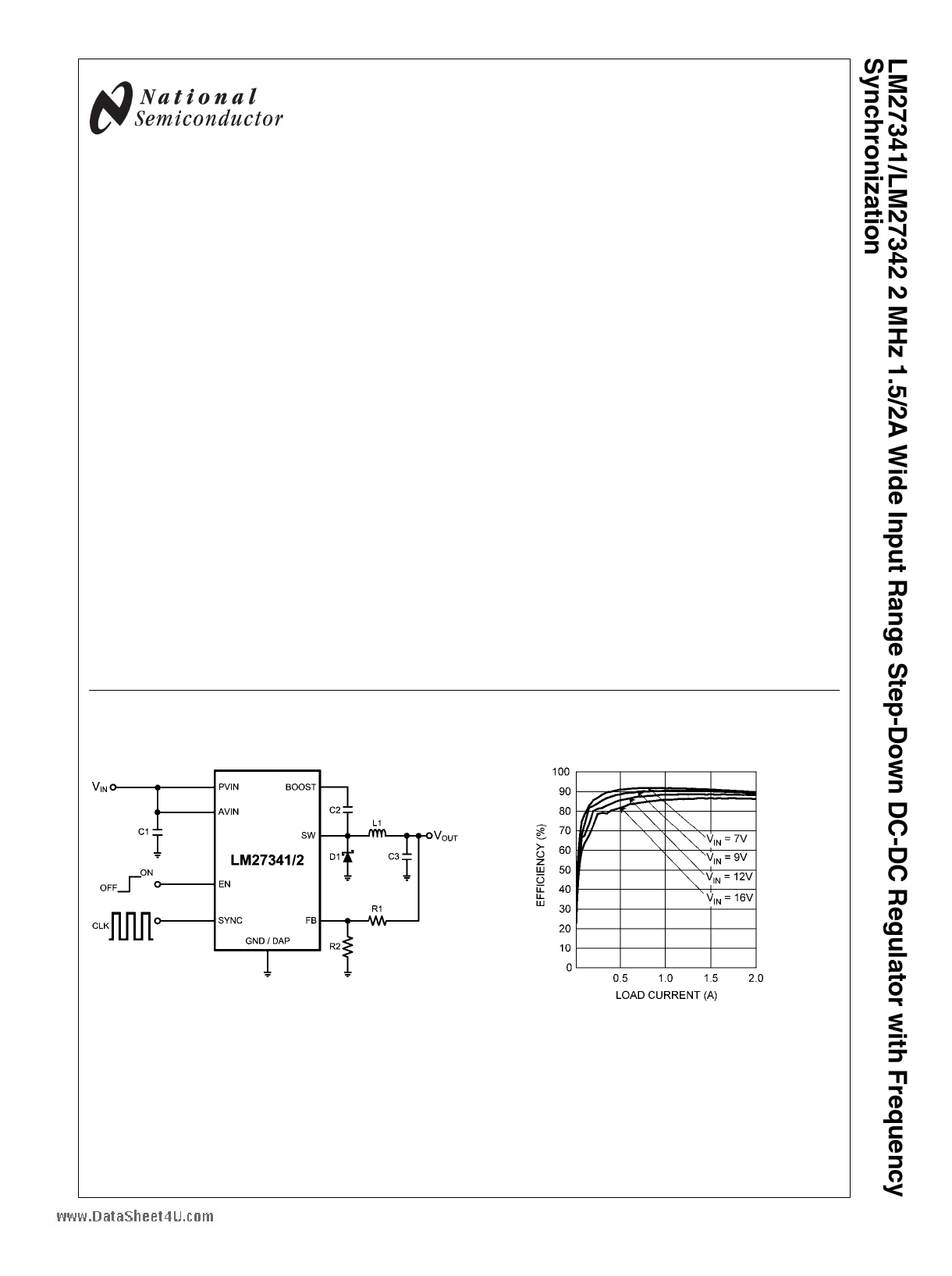
Typical Application Circuit
30005674
30005676
Efficiency vs Load Current
VOUT = 5V, fsw = 2 MHz
© 2008 National Semiconductor Corporation 300056
www.national.com
1 page 
Typical Performance Characteristics
TA = 25°C, unless specified otherwise.
All
curves
taken
at
VIN
=
12V,
VBOOST
-
VSW
= 4.3V and
www.DataSheet4U.com
Efficiency vs Load Current
VOUT = 5V, fSW = 2 MHz
Refer to Figure 10
Load Transient
VOUT = 5V, IOUT = 100 mA - 2A @ slewrate = 2A / µs
Refer to Figure 10
30005676
Efficiency vs Load Current
VOUT = 3.3V, fSW = 2 MHz
Refer to Figure 12
300056100
Load Transient
VOUT = 3.3V, IOUT = 100 mA - 2A @ slewrate = 2A / µs
Refer to Figure 12
30005680
Efficiency vs Load Current
VOUT = 1.8V, fSW = 2 MHz
Refer to Figure 15
300056102
Load Transient
VOUT = 1.8V, IOUT = 100 mA - 2A @ slewrate = 2A / µs
Refer to Figure 15
30005684
5
300056105
www.national.com
5 Page 
BOOST FUNCTION
Capacitor C2 in Figure 1, commonly referred to as CBOOST, is
used to store a voltage VBOOST. When the LM27341/LM27342
starts up, an internal LDO charges CBOOST ,via an internal
diode, to a voltage sufficient to turn the internal NMOS switch
on. The gate drive voltage supplied to the internal NMOS
switch is VBOOST - VSW.
During a normal switching cycle, when the internal NMOS
control switch is off (tOFF) (refer to Figure 2), VBOOST equals
VLDO minus the forward voltage of the internal diode (VD2). At
the same time the inductor current (iL) forward biases the
catch diode D1 forcing the SW pin to swing below ground by
the forward voltage drop of the catch diode (VD1). Therefore,
the voltage stored across CBOOST is
VBOOST - VSW = VLDO - VD2 + VD1
Thus,
VBOOST = VSW + VLDO - VD2 + VD1
When the NMOS switch turns on (tON), the switch pin rises to
VSW = VIN – (RDSON x IL),
reverse biasing D1, and forcing VBOOST to rise. The voltage
at VBOOST is then
VBOOST = VIN – (RDSON x IL) + VLDO – VD2 + VD1
which is approximately
VIN + VLDO- 0.4V
VBOOST has pulled itself up by its "bootstraps", or boosted to
a higher voltage.
LOW INPUT VOLTAGE CONSIDERATIONS
When the input voltage is below 5V and the duty cycle is
greater than 75 percent, the gate drive voltage developed
across CBOOST might not be sufficient for proper operation of
the NMOS switch. In this case, CBOOST should be charged via
an external Schottky diode attached to a 5V voltage rail, see
Figure 3. This ensures that the gate drive voltage is high
enough for proper operation of the NMOS switch in the triode
region. Maintain VBOOST - VSW less than the 6V absolute max-
imum rating.
www.DataSheet4U.com
30005636
FIGURE 4. Minimum Load Current for L = 1.5 µH
ENABLE PIN / SHUTDOWN MODE
Connect the EN pin to a voltage source greater than 1.8V to
enable operation of the LM27341/LM27342. Apply a voltage
less than 0.4V to put the part into shutdown mode. In shut-
down mode the quiescent current drops to typically 70 nA.
Switch leakage adds another 40 nA from the input supply. For
proper operation, the LM27341/LM27342 EN pin should nev-
er be left floating, and the voltage should never exceed VIN +
0.3V.
The simplest way to enable the operation of the LM27341/
LM27342 is to connect the EN pin to AVIN which allows self
start-up of the LM27341/LM27342 when the input voltage is
applied.
When the rise time of VIN is longer than the soft-start time of
the LM27341/LM27342 this method may result in an over-
shoot in output voltage. In such applications, the EN pin
voltage can be controlled by a separate logic signal, or tied to
a resistor divider, which reaches 1.8V after VIN is fully estab-
lished (see Figure 5). This will minimize the potential for
output voltage overshoot during a slow VIN ramp condition.
Use the lowest value of VIN , seen in your application when
calculating the resistor network, to ensure that the 1.8V min-
imum EN threshold is reached.
30005626
FIGURE 3. External Diode Charges CBOOST
HIGH OUTPUT VOLTAGE CONSIDERATIONS
When the output voltage is greater than 3.3V, a minimum load
current is needed to charge CBOOST, see Figure 4. The mini-
mum load current forward biases the catch diode D1 forcing
the SW pin to swing below ground. This allows CBOOST to
charge, ensuring that the gate drive voltage is high enough
for proper operation. The minimum load current depends on
many factors including the inductor value.
11
FIGURE 5. Resistor Divider on EN
30005608
www.national.com
11 Page | ||
| Páginas | Total 30 Páginas | |
| PDF Descargar | [ Datasheet LM27342.PDF ] | |
Hoja de datos destacado
| Número de pieza | Descripción | Fabricantes |
| LM2734 | Thin SOT23 1A Load Step-Down DC-DC Regulator | National Semiconductor |
| LM2734 | LM2734 Thin SOT 1-A Load Step-Down DC-DC Regulator (Rev. J) | Texas Instruments |
| LM2734-Q1 | LM2734 Thin SOT 1-A Load Step-Down DC-DC Regulator (Rev. J) | Texas Instruments |
| LM27341 | LM27341/2/1Q/2Q 2 MHz 1.5A/2A Wide Input Range Step-Down DC-DC Reg w/ Freq Sync (Rev. E) | Texas Instruments |
| Número de pieza | Descripción | Fabricantes |
| SLA6805M | High Voltage 3 phase Motor Driver IC. |
Sanken |
| SDC1742 | 12- and 14-Bit Hybrid Synchro / Resolver-to-Digital Converters. |
Analog Devices |
|
DataSheet.es es una pagina web que funciona como un repositorio de manuales o hoja de datos de muchos de los productos más populares, |
| DataSheet.es | 2020 | Privacy Policy | Contacto | Buscar |