|
|
|
PDF ZL2105 Data sheet ( Hoja de datos )
| Número de pieza | ZL2105 | |
| Descripción | 3A Integrated Digital DC-DC Converter | |
| Fabricantes | Intersil Corporation | |
| Logotipo | ||
Hay una vista previa y un enlace de descarga de ZL2105 (archivo pdf) en la parte inferior de esta página. Total 36 Páginas | ||
|
No Preview Available !
Data Sheet
3A Integrated Digital DC-DC Converter
Description
The ZL2105 is an innovative power conversion and
management IC that combines an integrated
synchronous step-down DC-DC converter with key
power management functions in a small package,
resulting in a flexible and integrated solution.
Zilker Labs Digital-DC™ technology enables
unparalleled power management integration while
delivering industry-leading performance in a tiny
footprint.
The ZL2105 can provide an output voltage from
0.6 V to 5.5 V from an input voltage between 4.5 V
and 14 V. Internal 4.5 A low RDS(ON) synchronous
power MOSFETs enable the ZL2105 to deliver
continuous loads up to 3 A with high efficiency,
and an internal Schottky bootstrap diode further
reduces discrete component count. The ZL2105
also supports phase spreading for reduced system
capacitance.
Power management features such as digital soft-
start delay and ramp, sequencing, tracking, and
margining can be configured by simple pin-
strapping or through an on-chip serial port. The
ZL2105 uses standard PMBus™ protocol for
communicating with other devices to provide
intelligent system power management.
ZL2105
www.DataSheet4U.com
February 18, 2009
FN6851.0
Features
Power Conversion
High efficiency
3 A continuous output current
Integrated MOSFET switches
4.5 V to 14 V input range
0.54 V to 5.5 V output range (with margin)
±1% output voltage accuracy
200 kHz to 2 MHz switching frequency
Supports phase spreading
Small footprint (6 x 6 mm QFN package)
Power Management
Digital soft start/stop
Precision delay and ramp-up
Power good/enable
Voltage tracking, sequencing, and margining
Output voltage/current monitoring
Thermal monitor w/ shutdown
Non-volatile memory
I2C/SMBus™ communication bus
PMBus compatible
Applications
Telecom and storage equipment
Digital set-top box
Industrial supplies
12 V distributed power systems
Point of load converters
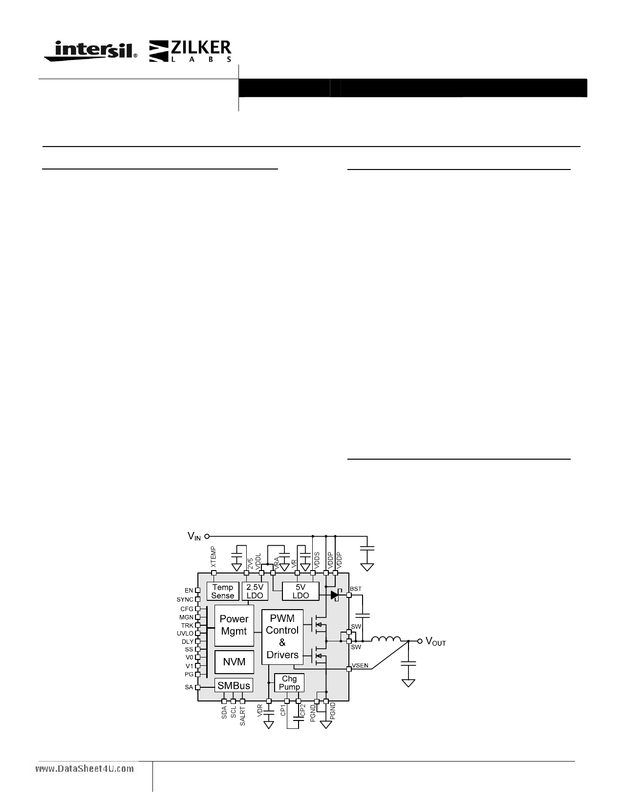
Figure 1. Block Diagram
1 1-888-INTERSIL or 1-888-468-3774|Intersil (and design) is a registered trademark of Intersil Americas Inc.
Copyright © Intersil Americas Inc. 2009. All Rights Reserved
All other trademarks mentioned are the property of their respective owners
1 page 
ZL2105
Table 3. Electrical Characteristics (continued)
www.DataSheet4U.com
VDDP = VDDS = 12 V, TA = -40°C to 85°C unless otherwise noted. Typical values are at TA = 25°C.
Parameter
Conditions
Min Typ Max
Unit
Oscillator and Switching Characteristics
Switch node current, ISW
Switching frequency range
Sourcing or Sinking
– 3 4.0 A
200 – 2000 kHz
Switching frequency set-point accuracy
Predefined settings
-5 –
5
%
Minimum SYNC pulse width
150 –
–
ns
Input clock frequency drift tolerance
External clock source
-13 –
13
%
Maximum duty cycle
90 –
–
%
RDS(ON) of High Side N-channel FETs
RDS(ON) of Low Side N-channel FETs
Fault Protection Characteristics
ISW = 1 A, VGS = 4.7 V
ISW=1A, VGS=8.5V, Charge Pump
ISW=1A, VGS=12V
–
–
–
125 180
123 140
114 130
mΩ
mΩ
mΩ
UVLO threshold range
3.79 – 13.2
V
UVLO setpoint accuracy
-2 –
2
%
UVLO hysteresis
Factory default
Configurable via I2C/SMBus
–3–
%
0 – 100 %
UVLO delay
– – 2.5 µs
Power good low threshold
Power good high threshold
Power good hysteresis
Power good delay
Factory default
Factory default
Factory default
Using pin-strap or resistor 1
Configurable via I2C/SMBus
– 90 – % VOUT
– 115 – % VOUT
–5–
%
0
– 200
ms
0 – 500 s
VSEN undervoltage threshold
VSEN overvoltage threshold
VSEN undervoltage hysteresis
VSEN undervoltage/ overvoltage fault
response time
Factory default
Configurable via I2C/SMBus
Factory default
Configurable via I2C/SMBus
Factory default
Configurable via I2C/SMBus
– 85 – % VOUT
0 – 110 % VOUT
– 115 – % VOUT
0 – 115 % VOUT
– 5 – % VO
– 16 –
µs
5 – 60 µs
Peak current limit threshold
Current limit setpoint accuracy
Current limit shutdown delay
Thermal protection threshold (junction
temperature)
0.2 – 4.5
Using ILIM pin or via I2C/SMBus – ±100 –
Factory default
–5–
Configurable via I2C/SMBus
1 – 32
Factory default
– 125 –
Configurable via I2C/SMBus
-40 – 125
A
mA
tSW 2
tSW 2
°C
°C
Thermal protection hysteresis
– 15 –
°C
Notes:
1. Factory default Power Good delay is set to the same value as the soft start ramp time.
2. tSW = 1/fSW, where fSW is the switching frequency.
5 Data Sheet Revision 2/18/2009
www.intersil.com
5 Page 
4.2 Power Conversion Overview
>
ZL2105
INPUT VOLTAGE BUS
www.DataSheet4U.com
>
PG EN MGN ILIM DLY SS CFG V(0,1)
VTRK
POWER MANAGEMENT NVM
ISENSE
LDO
BST
FC
SYNC
SALRT
SDA
SCL
SA
DDIIGGIITTAALL
CCOOMMPPEENNSSAATTOORR
D-PWM
SYNC
GEN
PLL
NLR
ADC
RESET
REF
ADC
COMMUNICATION
ADC
MUX
MOSFET
DRIVERS
Σ-
+
VDD
ISENSE
VR
TEMP
SENSOR
SW
VDR
CHG
PUMP
CP1
CP2
VSEN
XTEMP
VOUT
Figure 5. ZL2105 Block Diagram
The ZL2105 operates as a voltage-mode, synchronous
buck converter with a selectable constant frequency
PWM control scheme. The ZL2105 incorporates dual
low RDS(ON) synchronous MOSFETs to help minimize
the required circuit footprint.
Figure 6. Synchronous Buck Converter
Figure 6 illustrates the basic synchronous buck
converter topology showing the primary power train
components. This converter is also called a step-down
converter, as the output voltage must always be lower
than the input voltage. The ZL2105 integrates two
MOSFETs; QH is the top control MOSFET and QL is
the bottom synchronous MOSFET. The amount of time
that QH is on as a fraction of the total switching period
is known as the duty cycle D, which is described by the
following equation:
D
=
VOUT
VIN
During time D, QH is on and VIN – VOUT is applied
across the inductor.
As shown in Figure 5, the output voltage is directly
applied to the VSEN pin. The VSEN signal is then
compared to an internal programmable reference
voltage that is set to the desired output voltage level.
The error signal derived from this comparison is
converted to a digital value with a fast analog to digital
(A/D) converter. The digital signal is also applied to an
adjustable digital compensation filter, and the
compensated signal is used to derive the appropriate
PWM duty cycle for driving the internal MOSFETs.
The ZL2105 also incorporates a non-linear response
(NLR) loop to improve the response time and reduce
the output deviation as a result of a load transient. The
ZL2105 monitors the power converter’s operating
conditions and continuously adjusts the turn-on and
turn-off timing of the high-side and low-side
MOSFETs to optimize the overall efficiency of the
power supply.
11 Data Sheet Revision 2/18/2009
www.intersil.com
11 Page | ||
| Páginas | Total 36 Páginas | |
| PDF Descargar | [ Datasheet ZL2105.PDF ] | |
Hoja de datos destacado
| Número de pieza | Descripción | Fabricantes |
| ZL2101 | 6A Digital Synchronous Step-Down DC/DC Converter | Intersil Corporation |
| ZL2102 | 6A Digital Integrated Synchronous Step-Down DC/DC Regulator | Intersil |
| ZL2103 | 3A Digital-DC Synchronous Step-Down DC/DC Converter | Intersil Corporation |
| ZL2105 | 3A Integrated Digital DC-DC Converter | Intersil Corporation |
| Número de pieza | Descripción | Fabricantes |
| SLA6805M | High Voltage 3 phase Motor Driver IC. |
Sanken |
| SDC1742 | 12- and 14-Bit Hybrid Synchro / Resolver-to-Digital Converters. |
Analog Devices |
|
DataSheet.es es una pagina web que funciona como un repositorio de manuales o hoja de datos de muchos de los productos más populares, |
| DataSheet.es | 2020 | Privacy Policy | Contacto | Buscar |