|
|
PDF LTC6655 Data sheet ( Hoja de datos )
| Número de pieza | LTC6655 | |
| Descripción | Low Drift Precision References | |
| Fabricantes | Linear Technology | |
| Logotipo |  |
|
Hay una vista previa y un enlace de descarga de LTC6655 (archivo pdf) en la parte inferior de esta página. Total 26 Páginas | ||
|
No Preview Available !
LTC6655
0.25ppm Noise, Low Drift
Precision References
FEATURES
n Low Noise: 0.25ppmP-P (0.1Hz to 10Hz)
625nVP-P for the LTC6655-2.5
n Low Drift: 2ppm/°C Max
n High Accuracy: ±0.025% Max
n No Humidity Sensitivity (LS8 Package)
n Thermal Hysteresis (LS8): 30ppm (–40°C to 85°C)
n Long-Term Drift (LS8): 20ppm/√kHr
n 100% Tested at –40°C, 25°C and 125°C
n Load Regulation: <10ppm/mA
n Sinks and Sources Current: ±5mA
n Low Dropout: 500mV
n Maximum Supply Voltage: 13.2V
n Low Power Shutdown: <20µA Max
n Available Output Voltages: 1.25V, 2.048V, 2.5V, 3V,
3.3V, 4.096V, 5V
n Available in an 8-Lead MSOP and High Stability
Hermetic 5mm × 5mm LS8 Packages
APPLICATIONS
n Instrumentation and Test Equipment
n High Resolution Data Acquisition Systems
n Weigh Scales
n Precision Battery Monitors
n Precision Regulators
n Medical Equipment
DESCRIPTION
The LTC®6655 is a complete family of precision bandgap
voltage references, offering exceptional noise and drift
performance. This low noise and drift is ideally suited for
the high resolution measurements required by instrumenta-
tion and test equipment. In addition, the LTC6655 is fully
specified over the temperature range of –40°C to 125°C,
ensuring its suitability for demanding automotive and
industrial applications. Advanced curvature compensation
allows this bandgap reference to achieve a drift of less than
2ppm/°C with a predictable temperature characteristic
and an output voltage accurate to ±0.025%, reducing or
eliminating the need for calibration.
The LTC6655 can be powered from as little as 500mV
above the output voltage to as much as 13.2V. Superior
load regulation with source and sink capability, coupled
with exceptional line rejection, ensures consistent per-
formance over a wide range of operating conditions. A
shutdown mode is provided for low power applications.
The LTC6655 references are offered in an 8-lead MSOP
package and an 8-lead LS8 package. The LS8 is a 5mm
× 5mm surface mount hermetic package that provides
outstanding stability.
L, LT, LTC, LTM, Linear Technology and the Linear logo are registered trademarks of Linear
Technology Corporation. All other trademarks are the property of their respective owners.
TYPICAL APPLICATION
3V < VIN ≤ 13.2V
Basic Connection
CIN
0.1µF
LTC6655-2.5
VIN VOUT_F
SHDN
VOUT_S
GND
VOUT
COUT
10µF
6655 TA01a
Low Frequency 0.1Hz to 10Hz Noise (LTC6655-2.5)
500nV/DIV
For more information www.linear.com/LTC6655
1s/DIV
6655 TA01b
6655fe
1
1 page 
LTC6655
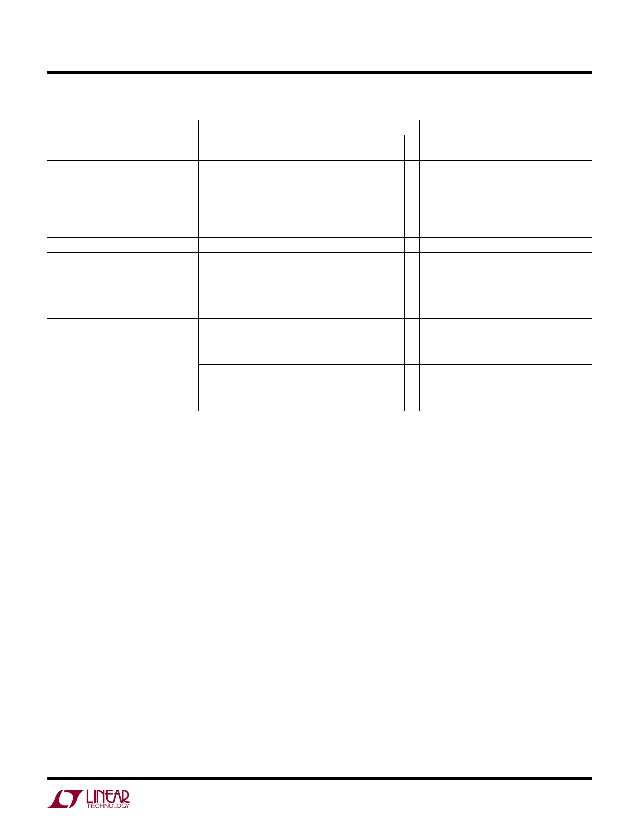
E LECTRICAL CHARACTERISTICS The l denotes the specifications which apply over the full operating
temperature range, otherwise specifications are at TA = 25°C. VIN = VOUT + 0.5V, VOUT_S connected to VOUT_F , unless otherwise noted.
PARAMETER
CONDITIONS
MIN TYP MAX
UNITS
Output Short-Circuit Current
Shutdown Pin (SHDN)
Short VOUT to GND
Short VOUT to VIN
Logic High Input Voltage
Logic High Input Current, SHDN = 2V
20
20
l 2.0
l
12
mA
mA
V
µA
Logic Low Input Voltage
Logic Low Input Current, SHDN = 0.8V
l
l
0.8 V
15 µA
Supply Current
No Load
57
mA
l 7.5 mA
Shutdown Current
SHDN Tied to GND
l 20 µA
Output Voltage Noise (Note 7)
0.1Hz ≤ f ≤ 10Hz
10Hz ≤ f ≤ 1kHz
Turn-On Time
0.1% Settling, COUT = 2.7µF
Long-Term Drift of Output Voltage (Note 8) LTC6655MS8
LTC6655LS8
0.25
0.67
ppppmmRPM-SP
400 µs
60 ppm/√kHr
20 ppm/√kHr
Hysteresis (Note 9)
LTC6655MS8
∆T = 0°C to 70°C
∆T = –40°C to 85°C
∆T = –40°C to 125°C
20 ppm
30 ppm
60 ppm
LTC6655LS8
∆T = 0°C to 70°C
∆T = –40°C to 85°C
∆T = –40°C to 125°C
5 ppm
30 ppm
80 ppm
Note 1: Stresses beyond those listed under Absolute Maximum Ratings
may cause permanent damage to the device. Exposure to any Absolute
Maximum Rating condition for extended periods may affect device
reliability and lifetime.
Note 2: Precision may be affected if the parts are stored outside of the
specified temperature range. Large temperature changes may cause
changes in device performance due to thermal hysteresis. For best
performance, extreme temperatures should be avoided whenever possible.
Note 3: The stated temperature is typical for soldering of the leads during
manual rework. For detailed IR reflow recommendations, refer to the
Applications Information section.
Note 4: Temperature coefficient is measured by dividing the maximum
change in output voltage by the specified temperature range.
Note 5: Load regulation is measured on a pulse basis from no load to
the specified load current. Load current does not include the 2mA sense
current. Output changes due to die temperature change must be taken into
account separately.
Note 6: Excludes load regulation errors. Minimum supply for the
LTC6655‑1.25, LTC6655-2.048 and LTC6655-2.5 is set by internal
circuitry supply requirements, regardless of load condition. Minimum
supply for the LTC6655-3, LTC6655-3.3, LTC6655-4.096 and LTC6655-5
is specified by load current.
Note 7: Peak-to-peak noise is measured with a 2-pole highpass filter at
0.1Hz and 3-pole lowpass filter at 10Hz. The unit is enclosed in a still-air
environment to eliminate thermocouple effects on the leads, and the
test time is 10 seconds. Due to the statistical nature of noise, repeating
noise measurements will yield larger and smaller peak values in a given
measurement interval. By repeating the measurement for 1000 intervals,
each 10 seconds long, it is shown that there are time intervals during
which the noise is higher than in a typical single interval, as predicted by
statistical theory. In general, typical values are considered to be those for
which at least 50% of the units may be expected to perform similarly or
better. For the 1000 interval test, a typical unit will exhibit noise that is
less than the typical value listed in the Electrical Characteristics table in
more than 50% of its measurement intervals. See Application Note 124 for
noise testing details. RMS noise is measured with a spectrum analyzer in a
shielded environment.
Note 8: Long-term stability typically has a logarithmic characteristic and
therefore, changes after 1000 hours tend to be much smaller than before
that time. Total drift in the second thousand hours is normally less than
one-third that of the first thousand hours with a continuing trend toward
reduced drift with time. Long-term stability is also affected by differential
stresses between the IC and the board material created during board
assembly.
Note 9: Hysteresis in output voltage is created by mechanical stress
that differs depending on whether the IC was previously at a higher or
lower temperature. Output voltage is always measured at 25°C, but
the IC is cycled to the hot or cold temperature limit before successive
measurements. Hysteresis is roughly proportional to the square of the
temperature change. For instruments that are stored at well controlled
temperatures (within 20 or 30 degrees of operational temperature),
hysteresis is usually not a significant error source. Typical hysteresis is the
worst case of 25°C to cold to 25°C or 25°C to hot to 25°C, preconditioned
by one thermal cycle.
For more information www.linear.com/LTC6655
6655fe
5
5 Page 
LTC6655
APPLICATIONS INFORMATION
Bypass and Load Capacitors
The LTC6655 voltage references require a 0.1µF or larger
input capacitor located close to the part to improve power
supply rejection. An output capacitor with a value between
2.7µF and 100µF is also required.
The output capacitor has a direct effect on the stability,
turn-on time and settling behavior. Choose a capacitor
with low ESR to insure stability. Resistance in series with
the output capacitor (ESR) introduces a zero in the output
buffer transfer function and could cause instability. The
2.7μF to 100μF range includes several types of capacitors
that are readily available as through-hole and surface mount
components. It is recommended to keep ESR less than or
equal to 0.1Ω. Capacitance and ESR are both frequency
dependent. At higher frequencies capacitance drops and
ESR increases. To insure stable operation the output ca-
pacitor should have the required values at 100kHz.
In order to achieve the best performance, caution should be
used when choosing a capacitor. X7R ceramic capacitors
are small, come in appropriate values and are relatively
stable over a wide temperature range. However, for a low
noise application X7R capacitors may not be suitable since
they may exhibit a piezoelectric effect. The mechanical
vibrations cause a charge displacement in the ceramic
dielectric and the resulting perturbation can look like noise.
If X7R capacitors are necessary, a thorough bench evalu-
ation should be completed to verify proper performance.
For very low noise applications where every nanovolt
counts, film capacitors should be considered for their
low noise and lack of piezoelectric effects. Film capaci-
tors such as polyester, polystyrene, polycarbonate, and
polypropylene have good temperature stability. Additional
care must be taken as polystyrene and polypropylene have
an upper temperature limit of 85°C to 105°C. Above these
temperatures, the working voltages need to be derated
according to manufacturer’s specifications. Another type
of film capacitor is polyphenylene sulfide (PPS). These
devices work over a wide temperature range, are stable,
and have large capacitance values beyond 1μF. In general,
film capacitors are found in surface mount and leaded
packages. Table 1 is a partial list of capacitor companies
and some of their available products.
In voltage reference applications, film capacitor lifetime
is affected by temperature and applied voltage. When
polyester capacitors are operated beyond their rated
temperatures (some capacitors are not rated for operation
above 85°C) they need to be derated. Voltage derating is
usually accomplished as a ratio of applied voltage to rated
voltage limit. Contact specific film capacitor manufactur-
ers to determine exact lifetime and derating information.
The lifetime of X7R capacitors is long, especially for
reference applications. Capacitor lifetime is degraded by
operating near or exceeding the rated voltage, at high
temperature, with AC ripple or some combination of these.
Most reference applications have AC ripple only during
transient events.
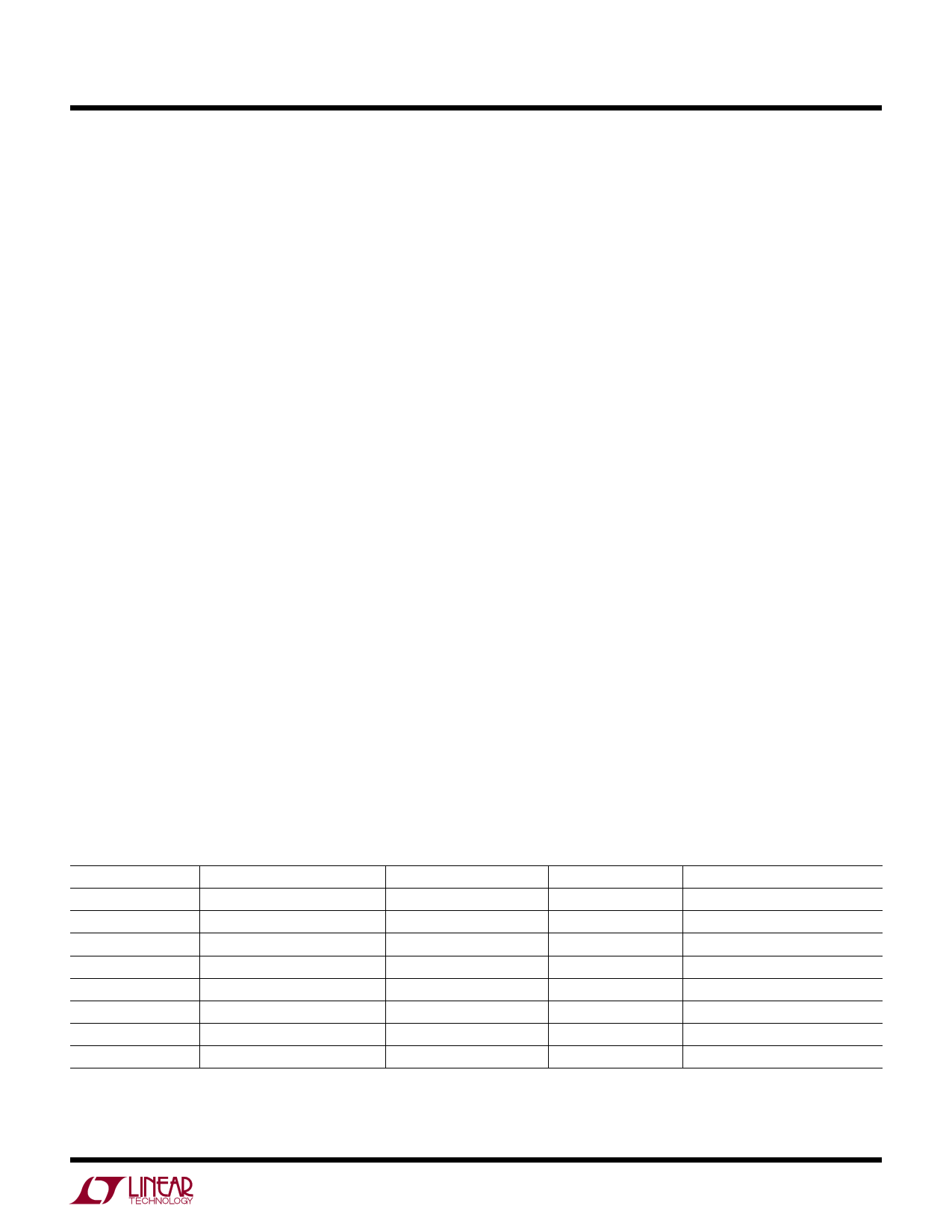
Table 1. Film Capacitor Companies
COMPANY
DIELECTRIC
Cornell Dublier
Polyester
Dearborn Electronics
Polyester
Tecate
Polyester
Wima
Polyester
Vishay
Polyester
Vishay
Polycarbonate
Dearborn Electronics
Polyphenylene Sulfide (PPS)
Wima
Polyphenylene Sulfide (PPS)
AVAILABLE CAPACITANCE
0.5µF to 10µF
0.1µF to 12µF
0.01µF to 18µF
10µF to 22µF
1000pF to 15µF
0.01µF to 10µF
0.01µF to 15µF
0.01µF to 6.8µF
TEMPERATURE RANGE
–55°C to 125°C
–55°C to 125°C
–40°C to 105°C
–55°C to 100°C
–55°C to 125°C
–55°C to 100°C
–55°C to 125°C
–55°C to 140°C
TYPE
DME
218P, 430P, 431P, 442P, and 410P
901, 914, and 914D
MKS 4, MKS 2-XL
MKT1820
MKC1862, 632P
820P, 832P, 842P, 860P, and 880P
SMD-PPS
For more information www.linear.com/LTC6655
6655fe
11
11 Page | ||
| Páginas | Total 26 Páginas | |
| PDF Descargar | [ Datasheet LTC6655.PDF ] | |
Hoja de datos destacado
| Número de pieza | Descripción | Fabricantes |
| LTC6652 | Precision Low Drift Low Noise Buffered Reference | Linear Technology |
| LTC6655 | Low Drift Precision References | Linear Technology |
| Número de pieza | Descripción | Fabricantes |
| SLA6805M | High Voltage 3 phase Motor Driver IC. |
Sanken |
| SDC1742 | 12- and 14-Bit Hybrid Synchro / Resolver-to-Digital Converters. |
Analog Devices |
|
DataSheet.es es una pagina web que funciona como un repositorio de manuales o hoja de datos de muchos de los productos más populares, |
| DataSheet.es | 2020 | Privacy Policy | Contacto | Buscar |
