|
|
|
PDF LC72346W Data sheet ( Hoja de datos )
| Número de pieza | LC72346W | |
| Descripción | Ultralow-Voltage ETR Controller with On-Chip LCD Driver | |
| Fabricantes | Sanyo Semicon Device | |
| Logotipo | ||
Hay una vista previa y un enlace de descarga de LC72346W (archivo pdf) en la parte inferior de esta página. Total 12 Páginas | ||
|
No Preview Available !
Ordering number : ENN*6651
Preliminary
CMOS IC
LC72346W, 72347W
Ultralow-Voltage ETR Controller
with On-Chip LCD Driver
Overview
The LC72346W and LC72347W are ultralow-voltage
electronic tuning microcontrollers that include a PLL that
operates up to 250 MHz and a 1/4 duty 1/2 bias LCD
driver on chip. This IC includes an on-chip DC-DC
converter that can easily create the power supply voltages
needed for electronic tuning and contribute to reducing
end product costs. This IC is optimal for portable audio
equipment that must operate from a single battery.
Function
• Program memory (ROM):
— 4096 × 16 bits (8K bytes) : LC72346
— 6144 × 16 bits (12K bytes): LC72347
• Data memory (RAM):
— 256 × 4 bits: LC72346
— 512 × 4 bits: LC72347
• Cycle time:
40 µs (all 1-word instructions) at 75kHz crystal oscillation
• Stack: 8 levels
• LCD driver: 48 to 80 segments (1/4 duty, 1/2 bias drive)
• Interrupts: Two external interrupts
Timer interrupts (1, 5, 10, and 50 ms)
• A/D converter:
Four input channels (6-bit successive approximation
conversion)
• Input ports: 7 ports (of which three can be switched for
use as A/D converter inputs)
• Output ports: 6 ports (of which 1 can be switched for use
as the beep tone output and 2 are open-drain ports)
• I/O ports: 20 ports (of which 8 can be switched for use
as LCD ports and as mask options, of which 3 can be
switched for use as serial I/O ports)
• Serial I/O: One system (LC72347)
• PLL: Reference frequencies:
1, 3, 3.125, 5, 6.25, 12.5, and 25 kHz
• Input frequencies: FM band: 10 to 250 MHz
AM band (high): 2 to 20 MHz
AM band (low): 0.5 to 10 MHz
• Input sensitivity:
FM band: 35 mVrms (50 mVrms at 130 MHz or higher
frequency)
AM band (high, low): 35 mVrms
• External reset input: During CPU and PLL operations,
instruction execution is started from location 0.
• Built-in power-on reset circuit:
The CPU starts execution from location 0 when power is
first applied.
• Halt mode: The controller-operating clock is stopped.
Continued on next page.
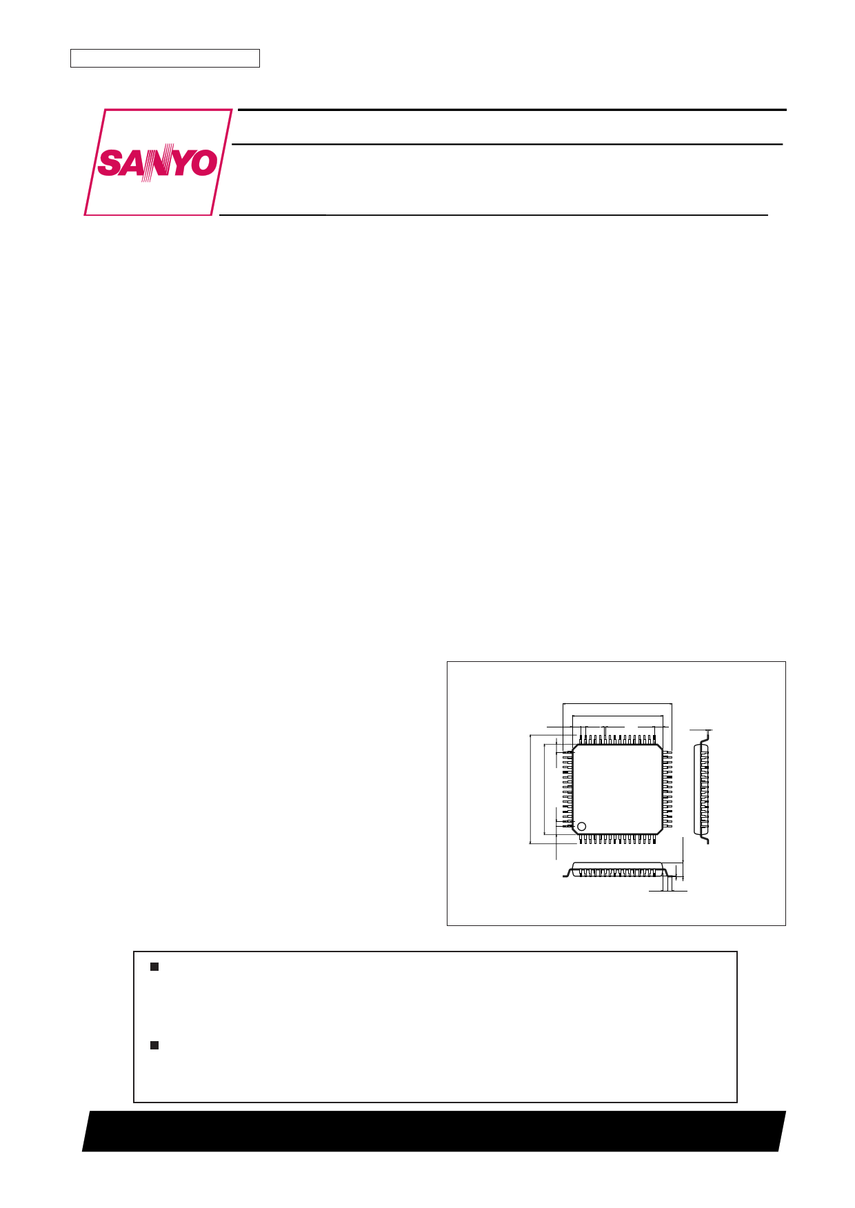
Package Dimensions
unit: mm
3190-SQFP64
[LC72346W, 72347W]
12.0
10.0
1.25 0.5 0.18
48
49
1.25
33
0.15
32
64
1
17
16
0.5 0.5
SANYO: SQFP64
Any and all SANYO products described or contained herein do not have specifications that can handle
applications that require extremely high levels of reliability, such as life-support systems, aircraft’s
control systems, or other applications whose failure can be reasonably expected to result in serious
physical and/or material damage. Consult with your SANYO representative nearest you before using
any SANYO products described or contained herein in such applications.
SANYO assumes no responsibility for equipment failures that result from using products at values that
exceed, even momentarily, rated values (such as maximum ratings, operating condition ranges, or other
parameters) listed in products specifications of any and all SANYO products described or contained
herein.
SANYO Electric Co.,Ltd. Semiconductor Company
TOKYO OFFICE Tokyo Bldg., 1-10, 1 Chome, Ueno, Taito-ku, TOKYO, 110-8534 JAPAN
N1501TN (OT) No. 6651-1/12
1 page 
LC72346W, 72347W
*1. Halt and PLL STOP mode current test circuit
*2. Backup mode current test circuit
7 pF
A
75 kHz
7 pF
XOUT VDD RES
XIN
PA, PF, PK
VSS
FMIN
AMIN
VDC3
VADJ
TEST1, 2
7 pF
75 kHz
A
XOUT VDD RES
XIN
7 pF
3V
VSS
FMIN
AMIN
VDC3
VADJ
TEST1, 2
3V
With all ports other than those specified above left open.
With output mode selected for PC and PD.
With segments S13 to S20 selected.
With all ports other than those specified above left open.
With output mode selected for PC and PD.
With segments S13 to S20 selected.
DC-DC Converter Application
VADJ
VDC3
VDDRAM
VDC1
VSS
VDD
No. 6651-5/12
5 Page 
LC72346W, 72347W
Continued from preceding page.
Mnemonic
AND
ANDI
OR
ORI
EXL
EXLI
SHR
LD
ST
MVRD
MVRS
MVSR
MVI
TMT
TMF
JMP
CAL
RT
RTI
SS
RS
TST
TSF
TUL
PLL
SIO
UCS
UCC
BEEP
DZC
TMS
IOS
IN
OUT
INR
OUTR
SPB
RPB
TPT
TPF
Operand
1st 2nd
Function
Operations function
Instruction format
f edcba9876543210
r M AND M with r
R ← (r) AND (M)
0 0 1 0 0 0 DH
DL
r
M I AND I with M
M ← (M) AND I
0 0 1 0 0 1 DH
DL
I
r M OR M with r
R ← (r) OR (M)
0 0 1 0 1 0 DH
DL
r
M I OR I with M
M ← (M) OR I
0 0 1 0 1 1 DH
DL
I
r M Exclusive OR M with r
R ← (r) XOR (M)
0 0 1 1 0 0 DH
DL
r
M I Exclusive OR M with M
M ← (M) XOR I
0 0 1 1 1 0 DH
DL
I
r Shift r right with carry
carry
(r)
000000001110
r
r M Load M to r
R ← (M)
1 1 0 1 0 0 DH
DL
r
M r Store r to M
M ← (r)
1 1 0 1 0 1 DH
DL
r
Move M to destination M
r M referring to r in the same row [DH, Rn] ← (M)
1 1 0 1 1 0 DH
DL
r
Move source M referring to r
M r to M in the same row
M ← [DH, Rn]
1 1 0 1 1 1 DH
DL
r
M1 M2 Move M to M in the same row [DH, DL1] ← [DH, DL2] 1 1 1 0 0 0 DH
DL1
DL2
M I Move I to M
M←I
1 1 1 0 0 1 DH
DL
I
Test M bits, then skip if all bits
M N specified are true
if M (N) = all 1, then skip 1 1 1 1 0 0 DH
DL
N
Test M bits, then skip if all bits
M N specified are false
if M (N) = all 0, then skip 1 1 1 1 0 1 DH
DL
N
ADDR Jump to the address
PC ← ADDR
100
ADDR (13 bits)
ADDR Call subroutine
PC ← ADDR
Stack ← (PC) + 1
101
ADDR (13 bits)
Return from subroutine
PC ← Stack
000000001000
Return from interrupt
PC ← Stack,
BANK ← Stack,
CARRY ← Stack
000000001001
SWR N Set status register
(Status W-reg) N ← 1
1 1 1 1 1 1 1 1 0 0 0 SWR
N
SWR N Reset status register
(Status W-reg) N ← 0
1 1 1 1 1 1 1 1 0 0 1 SWR
N
SRR N Test status register true
If (Status R-reg) N = all 1,
then skip
1
1
1
1
1
1
1
1
0
1
SRR
N
SRR N Test status register false
If (Status R-reg) N = all 0,
then skip
1 1 1 1 1 1 1 1 1 0 SRR
N
N Test Unlock F/F
If Unlock F/F (N) = All 0,
then skip
000000001101
N
M Load M to PLL register
PLL reg ← PLL data
1 1 1 1 1 0 DH
DL
r
I1 I2 Serial I/O control
SIO reg ← I1, I2
00000001
I1
I2
I Set I to UCCW1
UCCW1 ← I
000000000001
I
I Set I to UCCW2
UCCW2 ← I
000000000010
I
I Beep control
BEEP reg ← I
000000000110
I
I Dead zone control
DZC reg ← I
000000001011
I
I Set timer register
Timer reg ← I
000000001100
I
PWn N Set port control word
IOS reg PWn ← N
11111110
PWn
N
M Pn Input port data to M
M ← (Pn)
1 1 1 0 1 0 DH
DL
Pn
M Pn Output contents of M to port
Pn ← M
1 1 1 0 1 1 DH
DL
Pn
M Rn Input register/port data to M
M ← (Pn reg)
0 0 1 1 1 0 DH
DL
Pn
Output contents of M to
M Rn register/port
Rn reg ← (M)
0 0 1 1 1 1 DH
DL
Rn
N Set port1 bits
(Pn)N ← 1
00000010
Pn
N
N Reset port1 bits
(Pn)N ← 0
00000011
Pn
N
Test port1 bits, then skip if all bits
N specified are true
If (Pn)N = all 1, then skip 1 1 1 1 1 1 0 0
Pn
N
Test port1 bits, then skip if all bits
N specified are false
If (Pn)N = all 0, then skip 1 1 1 1 1 1 0 1
Pn
N
BANK
I Select Bank
BANK ← I
000000000111
I
Continued on next page.
No. 6651-11/12
11 Page | ||
| Páginas | Total 12 Páginas | |
| PDF Descargar | [ Datasheet LC72346W.PDF ] | |
Hoja de datos destacado
| Número de pieza | Descripción | Fabricantes |
| LC72346 | Ultralow-Voltage ETR Controller with On-Chip LCD Driver | Sanyo Semicon Device |
| LC723461W | (LC723461W / LC723462W) Ultralow-Voltage ETR Controller | Sanyo Semicon Device |
| LC723462W | (LC723461W / LC723462W) Ultralow-Voltage ETR Controller | Sanyo Semicon Device |
| LC72346W | Ultralow-Voltage ETR Controller with On-Chip LCD Driver | Sanyo Semicon Device |
| Número de pieza | Descripción | Fabricantes |
| SLA6805M | High Voltage 3 phase Motor Driver IC. |
Sanken |
| SDC1742 | 12- and 14-Bit Hybrid Synchro / Resolver-to-Digital Converters. |
Analog Devices |
|
DataSheet.es es una pagina web que funciona como un repositorio de manuales o hoja de datos de muchos de los productos más populares, |
| DataSheet.es | 2020 | Privacy Policy | Contacto | Buscar |