|
|
PDF IP3088CX15 Data sheet ( Hoja de datos )
| Número de pieza | IP3088CX15 | |
| Descripción | (IP3088CX5 - IP3088CX20) Passive LC-filter Network | |
| Fabricantes | NXP Semiconductors | |
| Logotipo | ||
Hay una vista previa y un enlace de descarga de IP3088CX15 (archivo pdf) en la parte inferior de esta página. Total 15 Páginas | ||
|
No Preview Available !
www.DataSheet4U.com
IP3088CX5; IP3088CX10;
IP3088CX15; IP3088CX20
Integrated 2, 4, 6 and 8-channel passive LC-filter network with
ESD protection to IEC 61000-4-2 level 4
Rev. 01 — 12 February 2010
Product data sheet
1. Product profile
1.1 General description
IP3088CX5, IP3088CX10, IP3088CX15 and IP3088CX20 is a 2, 4, 6 and 8-channel LC
low-pass filter array family which is designed to provide filtering of undesired RF signals
on the I/O ports of portable communication or computing devices. In addition, IP3088CX5,
IP3088CX10, IP3088CX15 and IP3088CX20 incorporates diodes to provide protection to
downstream components from ElectroStatic Discharge (ESD) voltages as high as ±15 kV
according IEC 61000-4-2 level 4.
The devices are fabricated using monolithic silicon technology and integrate and
incorporate up to 16 coils and 24 diodes in a 0.5 mm pitch Wafer-Level Chip-Scale
Package (WLCSP).
1.2 Features and benefits
Pb-free, RoHS compliant and free of halogen and antimony (Dark Green compliant)
Integrated 2, 4, 6 and 8-channel π-type LC-filter network
18 Ω channel series resistance; ≤ 45 pF (at 2.5 V DC) channel capacitance
Integrated ESD protection withstanding ±15 kV contact discharge, far exceeding
IEC 61000-4-2 level 4
ESD protection to ±30 kV contact discharge, per MIL-STD-883D, Method 3015
WLCSP with 0.5 mm pitch
1.3 Applications
Cellular and Personal Communication System (PCS) mobile handsets
Cordless telephones
Wireless data (WAN/LAN) systems and PDAs
1 page 
NXP Semiconductors
IP3088CX5/CX10/CwwXw.D1a5taS/hCeet4XU.c2om0
2, 4, 6 and 8-channel passive LC-filter network with ESD protection
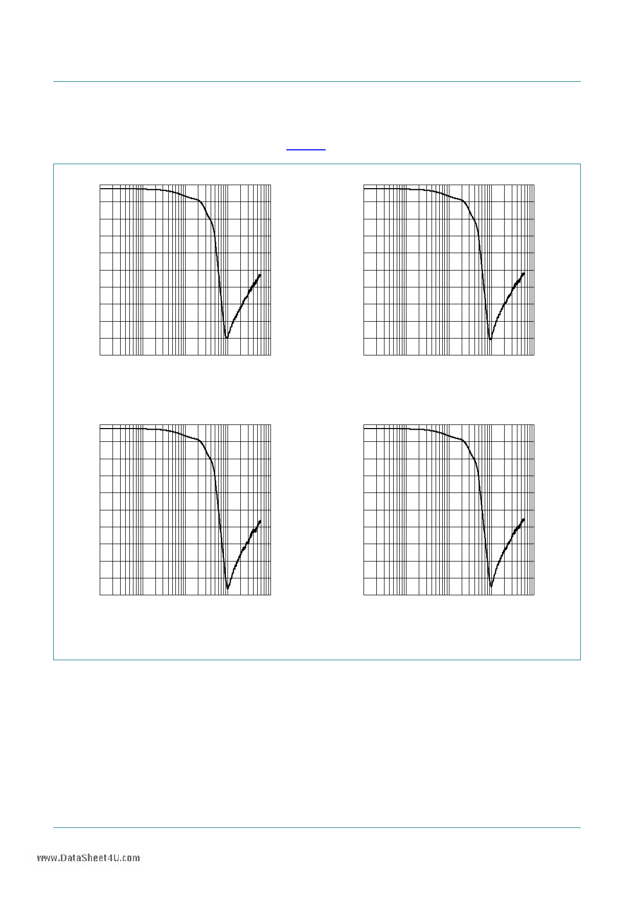
As an example, the measured insertion loss magnitude for all channels of the
IP3088CX10 are shown in Figure 7.
0
s21
(dB)
−10
001aak295
0
s21
(dB)
−10
001aak296
−20 −20
−30 −30
−40 −40
−50
1
10 102 103 104
f (MHz)
a. Channel 1 (pins A1 and C1)
0
s21
(dB)
−10
001aak294
−50
1
10 102 103 104
f (MHz)
b. Channel 2 (pins A2 and C2)
0
s21
(dB)
−10
001aak297
−20 −20
−30 −30
−40 −40
−50
1
10 102 103 104
f (MHz)
c. Channel 3 (pins A3 and C3)
Fig 7. Measured insertion loss magnitude
−50
1
10 102 103 104
f (MHz)
d. Channel 4 (pins A4 and C4)
IP3088CX5_CX10_CX15_CX20_1
Product data sheet
All information provided in this document is subject to legal disclaimers.
Rev. 01 — 12 February 2010
© NXP B.V. 2010. All rights reserved.
5 of 15
5 Page 
NXP Semiconductors
IP3088CX5/CX10/CwwXw.D1a5taS/hCeet4XU.c2om0
2, 4, 6 and 8-channel passive LC-filter network with ESD protection
temperature
maximum peak temperature
= MSL limit, damage level
minimum peak temperature
= minimum soldering temperature
peak
temperature
MSL: Moisture Sensitivity Level
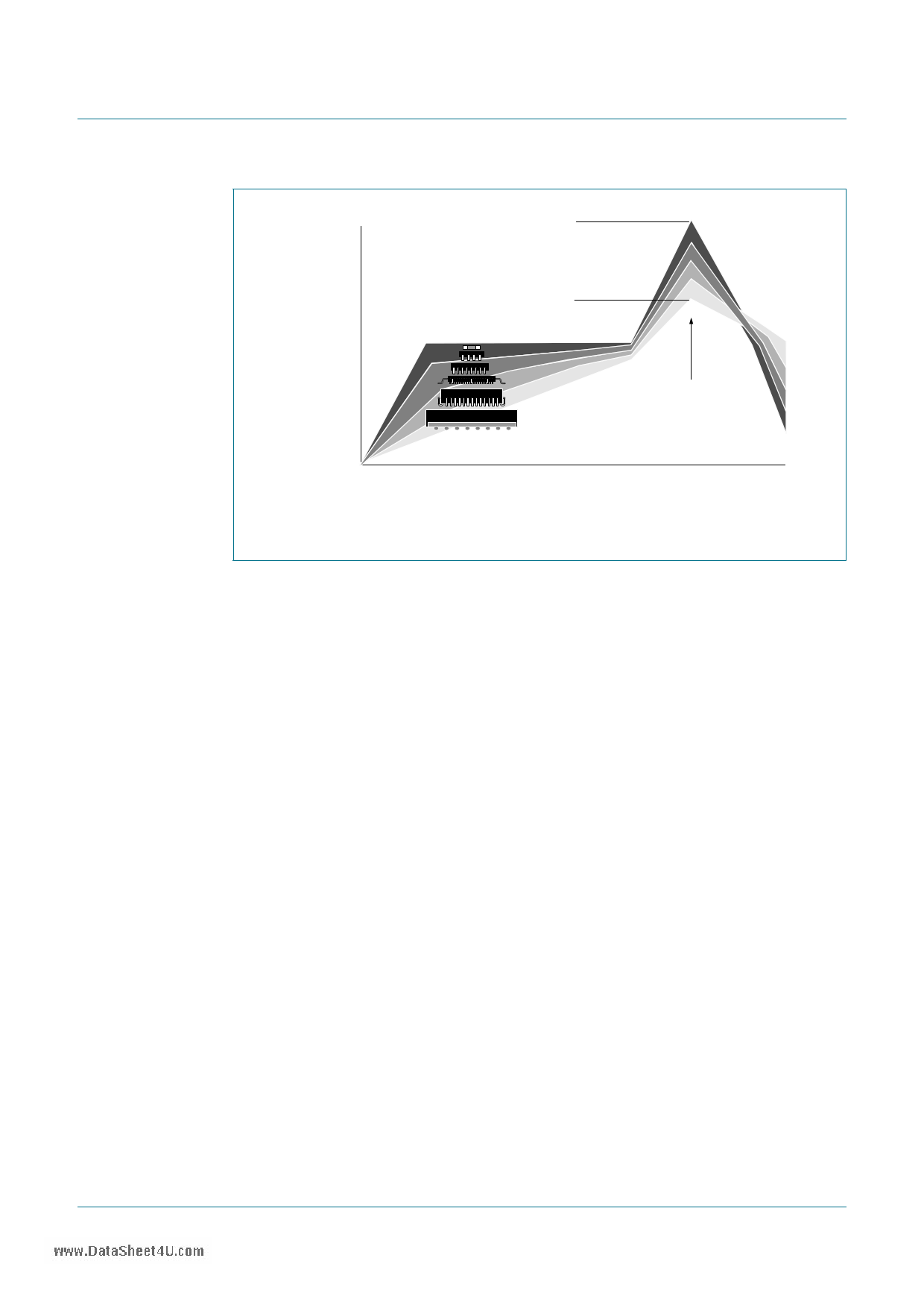
Fig 12. Temperature profiles for large and small components
time
001aac844
For further information on temperature profiles, refer to application note AN10365
“Surface mount reflow soldering description”.
9.3.1 Stand off
The stand off between the substrate and the chip is determined by:
• The amount of printed solder on the substrate
• The size of the solder land on the substrate
• The bump height on the chip
The higher the stand off, the better the stresses are released due to TEC (Thermal
Expansion Coefficient) differences between substrate and chip.
9.3.2 Quality of solder joint
A flip-chip joint is considered to be a good joint when the entire solder land has been
wetted by the solder from the bump. The surface of the joint should be smooth and the
shape symmetrical. The soldered joints on a chip should be uniform. Voids in the bumps
after reflow can occur during the reflow process in bumps with high ratio of bump diameter
to bump height, i.e. low bumps with large diameter. No failures have been found to be
related to these voids. Solder joint inspection after reflow can be done with X-ray to
monitor defects such as bridging, open circuits and voids.
9.3.3 Rework
In general, rework is not recommended. By rework we mean the process of removing the
chip from the substrate and replacing it with a new chip. If a chip is removed from the
substrate, most solder balls of the chip will be damaged. In that case it is recommended
not to re-use the chip again.
IP3088CX5_CX10_CX15_CX20_1
Product data sheet
All information provided in this document is subject to legal disclaimers.
Rev. 01 — 12 February 2010
© NXP B.V. 2010. All rights reserved.
11 of 15
11 Page | ||
| Páginas | Total 15 Páginas | |
| PDF Descargar | [ Datasheet IP3088CX15.PDF ] | |
Hoja de datos destacado
| Número de pieza | Descripción | Fabricantes |
| IP3088CX10 | (IP3088CX5 - IP3088CX20) Passive LC-filter Network | NXP Semiconductors |
| IP3088CX15 | (IP3088CX5 - IP3088CX20) Passive LC-filter Network | NXP Semiconductors |
| Número de pieza | Descripción | Fabricantes |
| SLA6805M | High Voltage 3 phase Motor Driver IC. |
Sanken |
| SDC1742 | 12- and 14-Bit Hybrid Synchro / Resolver-to-Digital Converters. |
Analog Devices |
|
DataSheet.es es una pagina web que funciona como un repositorio de manuales o hoja de datos de muchos de los productos más populares, |
| DataSheet.es | 2020 | Privacy Policy | Contacto | Buscar |
