|
|
|
PDF ADSP-BF547 Data sheet ( Hoja de datos )
| Número de pieza | ADSP-BF547 | |
| Descripción | High Performance Convergent Multimedia Blackfin Processor | |
| Fabricantes | Analog Devices | |
| Logotipo | ||
Hay una vista previa y un enlace de descarga de ADSP-BF547 (archivo pdf) en la parte inferior de esta página. Total 30 Páginas | ||
|
No Preview Available !
•
Blackfinwww.DataSheet4U.com
Embedded Processor
ADSP-BF542/ADSP-BF544/ADSP-BF547/ADSP-BF548/ADSP-BF549
FEATURES
Up to 600 MHz high-performance Blackfin processor
Two 16-bit MACs, two 40-bit ALUs, four 8-bit video ALUs
RISC-like register and instruction model
Wide range of operating voltages and flexible booting
options
Programmable on-chip voltage regulator
400-ball CSP_BGA, RoHS compliant package
MEMORY
Up to 324K bytes of on-chip memory comprised of
instruction SRAM/cache; dedicated instruction SRAM; data
SRAM/cache; dedicated data SRAM; scratchpad SRAM
External sync memory controller supporting either DDR
SDRAM or mobile DDR SDRAM
External async memory controller supporting 8-/16-bit async
memories and burst flash devices
NAND flash controller
4 memory-to-memory DMA pairs, 2 with ext. requests
Memory management unit providing memory protection
Code security with Lockbox® secure technology and 128-bit
AES/ ARC4 data encryption
One-time-programmable (OTP) memory
PERIPHERALS
High-speed USB On-the-Go (OTG) with integrated PHY
SD/SDIO controller
ATA/ATAPI-6 controller
Up to 4 synchronous serial ports (SPORTs)
Up to 3 serial peripheral interfaces (SPI-compatible)
Up to 4 UARTs, two with automatic H/W flow control
Up to 2 CAN (controller area network) 2.0B interfaces
Up to 2 TWI (2-wire interface) controllers
8- or 16-bit asynchronous host DMA interface
Multiple enhanced parallel peripheral interfaces (EPPIs),
supporting ITU-R BT.656 video formats and 18-/24-bit LCD
connections
Media transceiver (MXVR) for connection to a MOST network
Pixel compositor for overlays, alpha blending, and color
conversion
Up to eleven 32-bit timers/counters with PWM support
Real-time clock (RTC) and watchdog timer
Up/down counter with support for rotary encoder
Up to 152 general-purpose I/O (GPIOs)
On-chip PLL capable of 0.5× to 64× frequency multiplication
Debug/JTAG interface
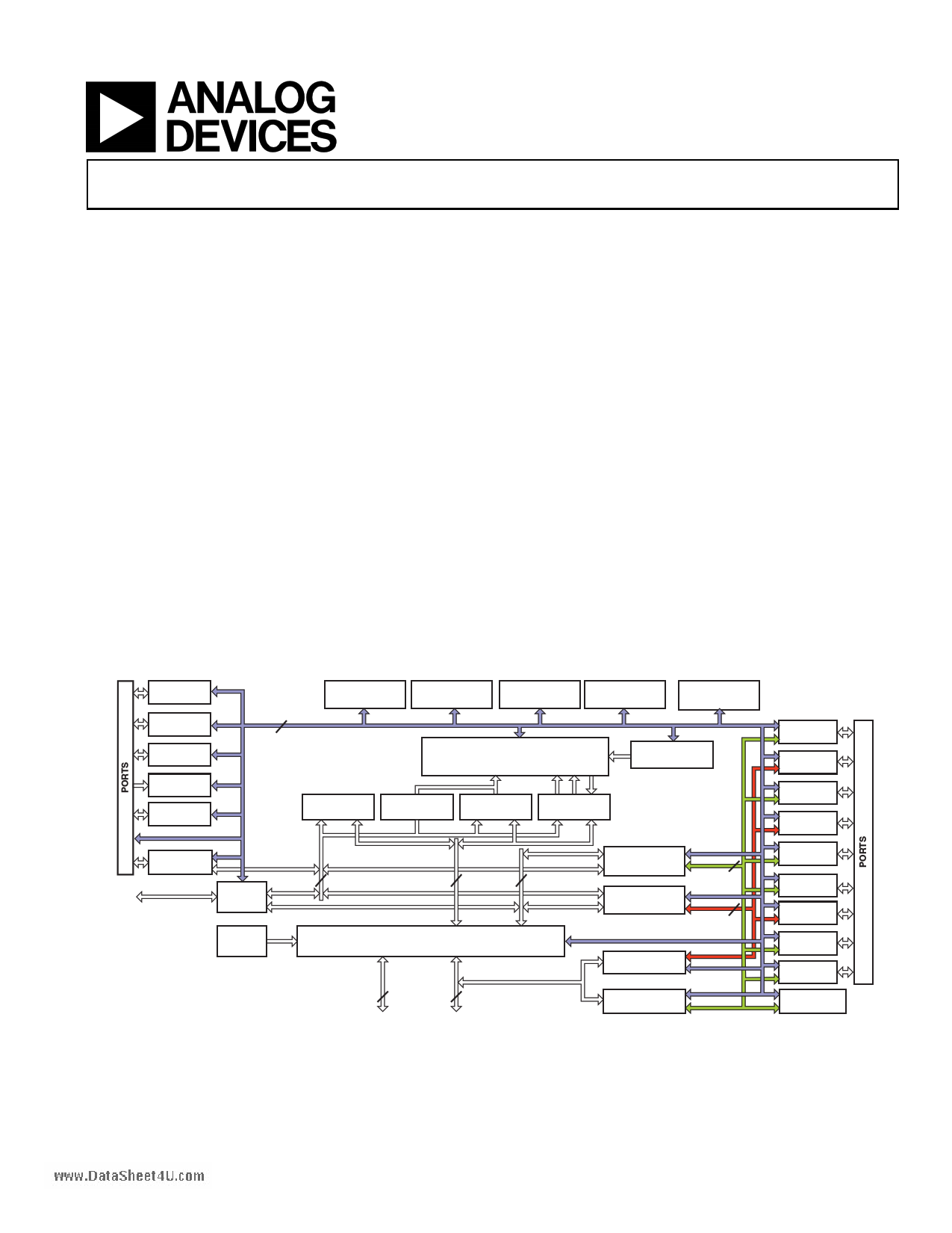
CAN (0-1)
TWI (0-1)
TIMERS(0-10)
COUNTER
KEYPAD
PAB 16
VOLTAGE
REGULATOR
JTAG TEST AND
EMULATION
RTC
B
WATCHDOG
TIMER
OTP
INTERRUPTS
L2
SRAM
L1
INSTR ROM
L1
INSTR SRAM
L1
DATA SRAM
MXVR
USB
DCB 32
EAB 64
DEB 32
BOOT
ROM
EXTERNAL PORT
NOR, DDR, MDDR
DDR/MDDR
16
ASYNC
16
32-BIT DMA
16-BIT DMA
DAB1 32
DAB0 16
ATAPI
NAND FLASH
CONTROLLER
HOST DMA
UART (0-1)
UART (2-3)
SPI (0-1)
SPI (2)
SPORT (2-3)
SPORT (0-1)
SD / SDIO
EPPI (0-2)
PIXEL
COMPOSITOR
Figure 1. ADSP-BF549 Functional Block Diagram
Blackfin and the Blackfin logo are registered trademarks of Analog Devices, Inc.
Rev. B
Information furnished by Analog Devices is believed to be accurate and reliable.
However, no responsibility is assumed by Analog Devices for its use, nor for any
infringements of patents or other rights of third parties that may result from its use.
Specifications subject to change without notice. No license is granted by implication
or otherwise under any patent or patent rights of Analog Devices. Trademarks and
registered trademarks are the property of their respective owners.
One Technology Way, P.O.Box 9106, Norwood, MA 02062-9106 U.S.A.
Tel:781/329-4700
www.analog.com
Fax:781/461-3113 © 2009 Analog Devices, Inc. All rights reserved.
1 page 
ADSP-BF542/ADSP-BF544/ADSP-BF547/ADSP-BFw5w4w.8Da/AtaDShSeePt4-UB.coFm549
length, and base registers (for circular buffering), and eight
additional 32-bit pointer registers (for C-style indexed stack
manipulation).
Blackfin processors support a modified Harvard architecture in
combination with a hierarchical memory structure. Level 1 (L1)
memories are those that typically operate at the full processor
speed with little or no latency. At the L1 level, the instruction
memory holds instructions only. The two data memories hold
data, and a dedicated scratchpad data memory stores stack and
local variable information.
In addition, multiple L1 memory blocks are provided, offering a
configurable mix of SRAM and cache. The memory manage-
ment unit (MMU) provides memory protection for individual
tasks that may be operating on the core and can protect system
registers from unintended access.
The architecture provides three modes of operation: user mode,
supervisor mode, and emulation mode. User mode has
restricted access to certain system resources, thus providing a
protected software environment, while supervisor mode has
unrestricted access to the system and core resources.
The Blackfin processor instruction set has been optimized so
that 16-bit opcodes represent the most frequently used instruc-
tions, resulting in excellent compiled code density. Complex
DSP instructions are encoded into 32-bit opcodes, representing
fully featured multifunction instructions. Blackfin processors
support a limited multi-issue capability, where a 32-bit instruc-
tion can be issued in parallel with two 16-bit instructions,
allowing the programmer to use many of the core resources in a
single instruction cycle.
The Blackfin processor assembly language uses an algebraic syn-
tax for ease of coding and readability. The architecture has been
optimized for use in conjunction with the C/C++ compiler,
resulting in fast and efficient software implementations.
ADDRESS ARITHMETIC UNIT
DA1 32
DA0 32
I3 L3 B3
I2 L2 B2
I1 L1 B1
I0 L0 B0
M3
M2
M1
M0
DAG1
32
RAB
DAG0
SP
FP
P5
P4
P3
P2
P1
P0
32
PREG
SD 32
LD1 32
LD0 32
32
32
R7.H
R6.H
R5.H
R4.H
R3.H
R2.H
R1.H
R0.H
R7.L
R6.L
R5.L
R4.L
R3.L
R2.L
R1.L
R0.L
8
BARREL
SHIFTER
16
40
A0
88
40 40
32 32
DATA ARITHMETIC UNIT
ASTAT
16
8
40
A1
Figure 2. Blackfin Processor Core
SEQUENCER
ALIGN
DECODE
LOOP BUFFER
CONTROL
UNIT
Rev. B | Page 5 of 112 | February 2009
5 Page 
ADSP-BF542/ADSP-BF544/ADSP-BF547/ADSP-BFw5w4w.8Da/AtaDShSeePt4-UB.coFm549
The ADSP-BF54x Blackfin processors’ DMA controllers sup-
port both 1-dimensional (1D) and 2-dimensional (2D) DMA
transfers. DMA transfer initialization can be implemented from
registers or from sets of parameters called descriptor blocks.
The 2D DMA capability supports arbitrary row and column
sizes up to 64K elements by 64K elements, and arbitrary row
and column step sizes up to ±32K elements. Furthermore, the
column step size can be less than the row step size, allowing
implementation of interleaved data streams. This feature is
especially useful in video applications where data can be de-
interleaved on the fly.
Examples of DMA types supported by the ADSP-BF54x Black-
fin processors’ DMA controllers include:
• A single, linear buffer that stops upon completion
• A circular, auto-refreshing buffer that interrupts on each
full or fractionally full buffer
• 1D or 2D DMA using a linked list of descriptors
• 2D DMA using an array of descriptors, specifying only the
base DMA address within a common page
In addition to the dedicated peripheral DMA channels, the
DMAC1 and DMAC0 controllers each feature two memory
DMA channel pairs for transfers between the various memories
of the ADSP-BF54x Blackfin processors. This enables transfers
of blocks of data between any of the memories—including
external DDR, ROM, SRAM, and flash memory—with minimal
processor intervention. Like peripheral DMAs, memory DMA
transfers can be controlled by a very flexible descriptor-based
methodology or by a standard register-based autobuffer
mechanism.
The memory DMA channels of the DMAC1 controller
(MDMA2 and MDMA3) can be controlled optionally by the
external DMA request input pins. When used in conjunction
with the External Bus Interface Unit (EBIU), this handshaked
memory DMA (HMDMA) scheme can be used to efficiently
exchange data with block-buffered or FIFO-style devices con-
nected externally. Users can select whether the DMA request
pins control the source or the destination side of the memory
DMA. It allows control of the number of data transfers for
memory DMA. The number of transfers per edge is program-
mable. This feature can be programmed to allow memory DMA
to have an increased priority on the external bus relative to the
core.
Host DMA Port Interface
The host DMA port (HOSTDP) facilitates a host device external
to the ADSP-BF54x Blackfin processors to be a DMA master
and transfer data back and forth. The host device always masters
the transactions, and the processor is always a DMA slave
device.
The HOSTDP is enabled through the peripheral access bus.
Once the port has been enabled, the transactions are controlled
by the external host. The external host programs standard DMA
configuration words in order to send/receive data to any valid
internal or external memory location. The host DMA port con-
troller includes the following features:
• Allows an external master to configure DMA read/write
data transfers and read port status
• Uses a flexible asynchronous memory protocol for its
external interface
• Allows an 8- or 16-bit external data interface to the host
device
• Supports half-duplex operation
• Supports little/big endian data transfers
• Acknowledge mode allows flow control on host
transactions
• Interrupt mode guarantees a burst of FIFO depth host
transactions
REAL-TIME CLOCK
The ADSP-BF54x Blackfin processors’ real-time clock (RTC)
provides a robust set of digital watch features, including current
time, stopwatch, and alarm. The RTC is clocked by a 32.768 kHz
crystal external to the ADSP-BF54x Blackfin processors. The
RTC peripheral has dedicated power supply pins so that it can
remain powered up and clocked even when the rest of the pro-
cessor is in a low-power state. The RTC provides several
programmable interrupt options, including interrupt per sec-
ond, minute, hour, or day clock ticks, interrupt on
programmable stopwatch countdown, or interrupt at a pro-
grammed alarm time.
The 32.768 kHz input clock frequency is divided down to a 1 Hz
signal by a prescaler. The counter function of the timer consists
of four counters: a 60-second counter, a 60-minute counter, a
24-hour counter, and a 32,768-day counter.
When enabled, the alarm function generates an interrupt when
the output of the timer matches the programmed value in the
alarm control register. There are two alarms. The first alarm is
for a time of day. The second alarm is for a day and time of
that day.
The stopwatch function counts down from a programmed value
with one-second resolution. When the stopwatch is enabled and
the counter underflows, an interrupt is generated.
Like the other peripherals, the RTC can wake up the
ADSP-BF54x processor from sleep mode upon generation of
any RTC wakeup event. Additionally, an RTC wakeup event can
wake up the ADSP-BF54x processors from deep sleep mode,
and it can wake up the on-chip internal voltage regulator from
the hibernate state.
Rev. B | Page 11 of 112 | February 2009
11 Page | ||
| Páginas | Total 30 Páginas | |
| PDF Descargar | [ Datasheet ADSP-BF547.PDF ] | |
Hoja de datos destacado
| Número de pieza | Descripción | Fabricantes |
| ADSP-BF542 | (ADSP-BF54x) Embedded Processor | Analog Devices |
| ADSP-BF544 | (ADSP-BF54x) Embedded Processor | Analog Devices |
| ADSP-BF547 | High Performance Convergent Multimedia Blackfin Processor | Analog Devices |
| ADSP-BF548 | (ADSP-BF54x) Embedded Processor | Analog Devices |
| Número de pieza | Descripción | Fabricantes |
| SLA6805M | High Voltage 3 phase Motor Driver IC. |
Sanken |
| SDC1742 | 12- and 14-Bit Hybrid Synchro / Resolver-to-Digital Converters. |
Analog Devices |
|
DataSheet.es es una pagina web que funciona como un repositorio de manuales o hoja de datos de muchos de los productos más populares, |
| DataSheet.es | 2020 | Privacy Policy | Contacto | Buscar |