|
|
PDF VND5E050K-E Data sheet ( Hoja de datos )
| Número de pieza | VND5E050K-E | |
| Descripción | Double channel high side driver | |
| Fabricantes | STMicroelectronics | |
| Logotipo |  |
|
Hay una vista previa y un enlace de descarga de VND5E050K-E (archivo pdf) en la parte inferior de esta página. Total 30 Páginas | ||
|
No Preview Available !
VND5E050J-E
VND5E050K-E
Double channel high side driver for automotive applications
Features
Max supply voltage
Operating voltage range
Max On-State resistance (per ch.)
Current limitation (typ)
Off state supply current
VCC
VCC
RON
ILIMH
IS
(1) Typical value with all loads connected.
41V
4.5 to 28V
50 mΩ
27 A
2 µA(1)
■ General
– Inrush current active management by
power limitation
– Very low stand-by current
– 3.0V CMOS compatible inputs
– Optimized electromagnetic emissions
– Very low electromagnetic susceptibility
– In compliance with the 2002/95/EC
european directive
■ Diagnostic functions
– Open Drain status output
– On-state open load detection
– Off-state open load detection
– Output short to Vcc detection
www.DataShee–t4UO.covmerload and short to ground (power
limitation) indication
– Thermal shutdown indication
■ Protections
– Undervoltage shutdown
– Overvoltage clamp
– Load current limitation
– Self limiting of fast thermal transients
– Protection against loss of ground and loss
of VCC
– Over-temperature shutdown with
autorestart (thermal shutdown)
– Reverse battery protected(a)
– Electrostatic discharge protection
(a )See Application schematic on page 22.
PowerSSO-12
PowerSSO-24
Application
■ All types of resistive, inductive and capacitive
loads
Description
The VND5E050J-E and VND5E050K-E are
double channel high-side drivers manufactured in
the ST proprietary VIPower M0-5 technology
and housed in the tiny PowerSSO-12 and
PowerSSO-24 packages.
The VND5E050J-E and VND5E050K-E are
designed to drive automotive grounded loads
delivering protection, diagnostics and easy 3V
and 5V CMOS-compatible interface with any
microcontroller.
The devices integrate advanced protective
functions such as load current limitation, inrush
and overload active management by power
limitation, over-temperature shut-off with
auto-restart and over-voltage active clamp.
A dedicated active low digital status pin is
associated with every output channel in order to
provide Enhanced diagnostic functions including
fast detection of overload and short-circuit to
ground, over-temperature indication, short-circuit
to VCC diagnosis and ON & OFF state open-load
detection.
The diagnostic feedback of the whole device can
be disabled by pulling the STAT_DIS pin up, thus
allowing wired-ORing with other similar devices.
February 2008
Rev 1
1/40
www.st.com
40
1 page 
VND5E050J-E / VND5E050K-E
Block diagram and pin description
1 Block diagram and pin description
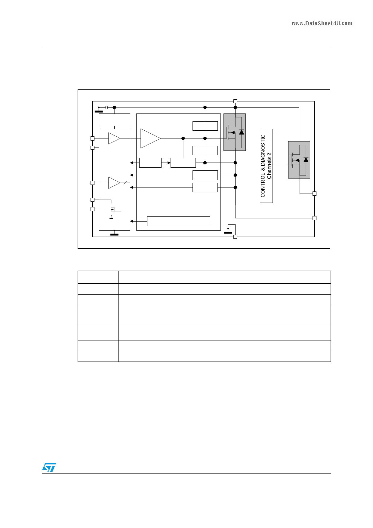
Figure 1. Block diagram
S ignal C lamp
U nde rvolta ge
IN1
IN2
S T_
D IS
S T1
S T2
LOG IC
C ontrol & Diagnostic 1
P ower
C lamp
DR IV E R
Over
temp.
C urrent
L imita tion
VON
L imita tion
OF F S tate
Open load
ON S tate
Open load
OVE R LOAD P R OTE C TION
(AC TIV E P OWE R LIMITATION)
VCC
CH 1
GND
CH 2
OUT2
OUT1
Table 1. Pin function
Name
Function
www.DataSheet4U.com
VCC
OUTPUTn
GND
INPUTn
STATUSn
STAT_DIS
Battery connection.
Power output.
Ground connection. Must be reverse battery protected by an external diode/resistor
network.
Voltage controlled input pin with hysteresis, CMOS compatible. Controls output
switch state.
Open Drain digital diagnostic pin.
Active high CMOS compatible pin, to disable the STATUS pin.
5/40
5 Page 
VND5E050J-E / VND5E050K-E
Electrical specifications
Table 9. Openload detection (8V<VCC<18V)
Symbol
Parameter
Test conditions
Min.
Openload ON state
IOL detection threshold
VIN = 5V;
10
tDOL(on)
tPOL
VOL
tDSTKON
Openload ON state
detection delay
IOUT = 0A, VCC=13V
(see Figure 4)
Delay between INPUT
falling edge and STATUS
rising edge in open load
condition
IOUT = 0A (see Figure 4)
Openload OFF state
voltage detection
threshold
VIN = 0V;
Output short circuit to
VCC detection delay at
turn Off
See Figure 4
200
2
180
IL(off2)
Off state output
current(1)
VIN= 0V; VOUT= 4V
(see Section 3.4: Open load
detection in Off state)
-75
td_vol
Delay response from
output rising edge to
STATUS falling edge in
open load
VIN= 0V; VOUT= 4V
(1) For each channel.
Typ.
500
Max. Unit
70 mA
200 µs
1200 µs
4V
tPOL µs
0 µA
20 µs
Table 10. Logic input
Symbol
Parameter
www.DataSheet4U.com
VIL
IIL
VIH
IIH
VI(hyst)
Input low level
Low level input current
Input high level
High level input current
Input hysteresis voltage
VICL Input clamp voltage
VSDL
ISDL
VSDH
ISDH
VSD(hyst)
STAT_DIS low level voltage
Low level STAT_DIS current
STAT_DIS high level voltage
High level STAT_DIS current
STAT_DIS hysteresis voltage
VSDCL STAT_DIS clamp voltage
Test conditions
VIN =0.9 V
VIN = 2.1 V
IIN = 1mA
IIN = -1mA
VSD = 0.9 V
VSD = 2.1 V
ISD=1mA
ISD=-1mA
Min. Typ. Max. Unit
1
2.1
0.25
5.5
-0.7
1
2.1
0.25
5.5
-0.7
0.9
10
7
0.9
10
7
V
µA
V
µA
V
V
V
V
µA
V
µA
V
V
V
11/40
11 Page | ||
| Páginas | Total 30 Páginas | |
| PDF Descargar | [ Datasheet VND5E050K-E.PDF ] | |
Hoja de datos destacado
| Número de pieza | Descripción | Fabricantes |
| VND5E050K-E | Double channel high side driver | STMicroelectronics |
| Número de pieza | Descripción | Fabricantes |
| SLA6805M | High Voltage 3 phase Motor Driver IC. |
Sanken |
| SDC1742 | 12- and 14-Bit Hybrid Synchro / Resolver-to-Digital Converters. |
Analog Devices |
|
DataSheet.es es una pagina web que funciona como un repositorio de manuales o hoja de datos de muchos de los productos más populares, |
| DataSheet.es | 2020 | Privacy Policy | Contacto | Buscar |
