|
|
|
PDF L6566B Data sheet ( Hoja de datos )
| Número de pieza | L6566B | |
| Descripción | Multi-mode controller | |
| Fabricantes | STMicroelectronics | |
| Logotipo | ||
Hay una vista previa y un enlace de descarga de L6566B (archivo pdf) en la parte inferior de esta página. Total 30 Páginas | ||
|
No Preview Available !
L6566B
Multi-mode controller for SMPS
Features
■ Selectable multi-mode operation:
fixed frequency or quasi-resonant
■ On-board 700 V high-voltage start-up
■ Advanced light load management
■ Low quiescent current (< 3 mA)
■ Adaptive UVLO
■ Line feedforward for constant power capability
vs mains voltage
■ Pulse-by-pulse OCP, shutdown on overload
(latched or autorestart)
■ Transformer saturation detection
■ Programmable frequency modulation for EMI
reduction
■ Latched or autorestart OVP
■ Brownout protection
■ -600/+800 mA totem pole gate driver with
active pull-down during UVLO
■ SO16N package
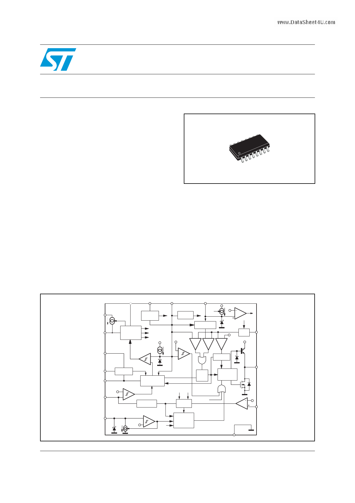
Figure 1. Block diagram
SO16N
Applications
■ Hi-end AC-DC adapter/charger
■ LCD TV/monitor, PDP
■ digital consumer, IT equipment
■ single-stage PFC
www.DataSheet4U.com
VREF
SS
COMP
VFF
1
HV
IHV
VCC
5
10 14
SOFT-START
&
FAULT MNGT
TIME
OUT
VOLTAGE
REGULATOR
&
ADAPTIVE UVLO
Ref erence
voltages
Internal supply
UVLO
VCC
9 15
LOW CLAMP OFF2
& DISABLE
VCC
OVP
LINE VOLTAGE
FEEDFORWARD
6.4V
Icharge
7.7V
OVPL
Q
LEB
1.5 V
7
-+ -+ +-
Vth
PWM
OCP
VCC
6
FMOD
UVLO_SHF
-
+
400 uA
5.7V
+
-
BURST-MODE
Hiccup-mode
OCP logic
OCP2
14V
4
OSC 13
OSCILLATOR
MODE/SC 12
ZCD
50 mV
100 mV
11
MODE SELECTION
&
TURN-ON LOGIC
ZERO CURRENT
- DETECTOR
+
OVERVOLTAGE
PROTECTION
OVP
R
Q
S
TIME
OUT OVPL
LATCH
OFF2
IC_LATCH
DRIVER
4.5V
8
AC_OK
16
3V
15 µA
0.450V
0.485V
-
+
AC_FAIL
UVLO
DISABLE
3
CS
GD
DIS
May 2008
Rev 2
1/51
www.st.com
51
1 page 
L6566B
List of figures
List of figures
Figure 1.
Figure 2.
Figure 3.
Figure 4.
Figure 5.
Figure 6.
Figure 7.
Figure 8.
Figure 9.
Figure 10.
Figure 11.
Figure 12.
Figure 13.
Figure 14.
Figure 15.
Figure 16.
Figure 17.
Figure 18.
Figure 19.
Figure 20.
Figure 21.
Figure 22.
Figure 23.
Figure 24.
Figure 25.
Figure 26.
Figure 27.
Figure 28.
Figure 29.
Figure 30.
www.DataSFhiegeut4reU.3co1m.
Figure 32.
Block diagram . . . . . . . . . . . . . . . . . . . . . . . . . . . . . . . . . . . . . . . . . . . . . . . . . . . . . . . . . . . . 1
Typical system block diagram. . . . . . . . . . . . . . . . . . . . . . . . . . . . . . . . . . . . . . . . . . . . . . . . 7
Pin connection (through top view) . . . . . . . . . . . . . . . . . . . . . . . . . . . . . . . . . . . . . . . . . . . . 8
Multi-mode operation with QR option active . . . . . . . . . . . . . . . . . . . . . . . . . . . . . . . . . . . . 17
High-voltage start-up generator: internal schematic . . . . . . . . . . . . . . . . . . . . . . . . . . . . . . 18
Timing diagram: normal power-up and power-down sequences . . . . . . . . . . . . . . . . . . . . 19
Timing diagram showing short-circuit behavior (SS pin clamped at 5V). . . . . . . . . . . . . . . 20
Zero current detection block, triggering block, oscillator block and related logic . . . . . . . . 20
Drain ringing cycle skipping as the load is gradually reduced . . . . . . . . . . . . . . . . . . . . . . 22
Operation of ZCD, triggering and oscillator blocks (QR option active) . . . . . . . . . . . . . . . . 23
Load-dependent operating modes: timing diagrams . . . . . . . . . . . . . . . . . . . . . . . . . . . . . 24
Addition of an offset to the current sense lowers the burst-mode operation threshold . . . . 25
Adaptive UVLO block. . . . . . . . . . . . . . . . . . . . . . . . . . . . . . . . . . . . . . . . . . . . . . . . . . . . . 25
Possible feedback configurations that can be used with the L6566B . . . . . . . . . . . . . . . . . 26
Externally controlled burst-mode operation by driving pin COMP: timing diagram. . . . . . . 27
Typical power capability change vs. input voltage in QR flyback converters . . . . . . . . . . . 28
Left: Overcurrent setpoint vs. VFF voltage; right: Line Feedforward function block . . . . . . 29
Hiccup-mode OCP: timing diagram . . . . . . . . . . . . . . . . . . . . . . . . . . . . . . . . . . . . . . . . . . 30
Frequency modulation circuit . . . . . . . . . . . . . . . . . . . . . . . . . . . . . . . . . . . . . . . . . . . . . . . 31
Operation after latched disable activation: timing diagram . . . . . . . . . . . . . . . . . . . . . . . . . 33
Soft-start pin operation under different operating conditions and settings . . . . . . . . . . . . . 34
OVP Function: internal block diagram . . . . . . . . . . . . . . . . . . . . . . . . . . . . . . . . . . . . . . . . 35
OVP function: timing diagram . . . . . . . . . . . . . . . . . . . . . . . . . . . . . . . . . . . . . . . . . . . . . . . 36
Maximum allowed duty cycle vs. switching frequency for correct OVP detection. . . . . . . . 37
Brownout protection: internal block diagram and timing diagram . . . . . . . . . . . . . . . . . . . . 38
Voltage sensing techniques to implement brownout protection with the L6566B . . . . . . . . 39
Slope compensation waveforms . . . . . . . . . . . . . . . . . . . . . . . . . . . . . . . . . . . . . . . . . . . . . 40
Typical low-cost application schematic . . . . . . . . . . . . . . . . . . . . . . . . . . . . . . . . . . . . . . . . 44
Typical full-feature application schematic (QR operation) . . . . . . . . . . . . . . . . . . . . . . . . . 44
Typical full-feature application schematic (FF operation) . . . . . . . . . . . . . . . . . . . . . . . . . . 45
Frequency foldback at light load (FF operation) . . . . . . . . . . . . . . . . . . . . . . . . . . . . . . . . 46
Latched shutdown upon mains overvoltage . . . . . . . . . . . . . . . . . . . . . . . . . . . . . . . . . . . . 46
5/51
5 Page 
L6566B
3 Electrical data
3.1
Maximum rating
Table 2. Absolute maximum ratings
Symbol
Pin
Parameter
VHVS
IHVS
VCC
VFMOD
Vmax
Vmax
IZCD
VMODE/SC
VOSC
PTOT
TSTG
TJ
1
1
5
6
7, 8, 10, 14
9, 15, 16
11
12
13
Voltage range (referred to ground)
Output current
IC supply voltage (Icc = 20 mA)
Voltage range
Analog inputs and outputs
Maximum pin voltage (Ipin ≤ 1 mA)
Zero current detector max. current
Voltage range
Voltage range
Power dissipation @TA = 50 °C
Storage temperature
Junction operating temperature range
3.2 Thermal data
Table 3. Thermal data
Symbol
Parameter
www.DataSheet4U.com
RthJA Thermal resistance junction to ambient
Electrical data
Value
-0.3 to 700
Self-limited
Self-limited
-0.3 to 2
-0.3 to 7
Self-limited
±5
-0.3 to 5.3
-0.3 to 3.3
0.75
-55 to 150
-40 to 150
Unit
V
V
V
mA
V
V
W
°C
°C
Value
120
Unit
°C/W
11/51
11 Page | ||
| Páginas | Total 30 Páginas | |
| PDF Descargar | [ Datasheet L6566B.PDF ] | |
Hoja de datos destacado
| Número de pieza | Descripción | Fabricantes |
| L6566 | The best light source is supported by the best electrode technology | Hamamatsu Corporation |
| L6566B | Multi-mode controller | STMicroelectronics |
| L6566BH | Multimode controller | STMicroelectronics |
| Número de pieza | Descripción | Fabricantes |
| SLA6805M | High Voltage 3 phase Motor Driver IC. |
Sanken |
| SDC1742 | 12- and 14-Bit Hybrid Synchro / Resolver-to-Digital Converters. |
Analog Devices |
|
DataSheet.es es una pagina web que funciona como un repositorio de manuales o hoja de datos de muchos de los productos más populares, |
| DataSheet.es | 2020 | Privacy Policy | Contacto | Buscar |