|
|
|
PDF ADAU1381 Data sheet ( Hoja de datos )
| Número de pieza | ADAU1381 | |
| Descripción | Low Noise Stereo Codec | |
| Fabricantes | Analog Devices | |
| Logotipo | ||
Hay una vista previa y un enlace de descarga de ADAU1381 (archivo pdf) en la parte inferior de esta página. Total 30 Páginas | ||
|
No Preview Available !
Low Noise Stereo Codec with Enhanced
Recording and Playback Processing
ADAU1381
FEATURES
GENERAL DESCRIPTION
24-bit stereo audio ADC and DAC
400 mW speaker amplifier (into 8 Ω load)
Built-in sound engine for audio processing
Wind noise detection and autofiltering
Enhanced stereo capture (ESC)
The ADAU1381 is a low power, 24-bit stereo audio codec. The
low noise DAC and ADC support sample rates from 8 kHz to
96 kHz. Low current draw and power saving modes make the
ADAU1381 ideal for battery-powered audio applications.
Dual-band automatic level control (ALC)
A configurable sound engine provides enhanced record and
6-band equalizer, including notch filter
playback processing to improve overall audio quality.
Sampling rates from 8 kHz to 96 kHz
Stereo pseudo differential microphone input
Optional stereo digital microphone input pulse-density
modulation (PDM)
Stereo line output
PLL supporting a range of input clock rates
Analog and digital I/O 1.8 V to 3.3 V
Software control via SigmaStudio graphical user interface
The record path includes two digital stereo microphone inputs
and an analog stereo input path. The analog inputs can be
configured for either a pseudo differential or a single-ended
stereo source. A dedicated analog beep input signal can be
mixed into any output path. The ADAU1381 includes a stereo
line output and speaker driver, which makes the device capable of
supporting dynamic speakers.
Software-controllable, clickless mute
Software register and hardware pin standby mode
32-lead, 5 mm × 5 mm LFCSP or 30-ball, 6 × 5 bump WLCSP
The serial control bus supports the I2C® or SPI protocols, and
the serial audio bus is programmable for I2S, left-justified, right-
justified, or TDM mode. A programmable PLL supports flexible
APPLICATIONS
clock generation for all standard rates and available master clocks
Digital still cameras
from 11 MHz to 20 MHz.
Digital video cameras
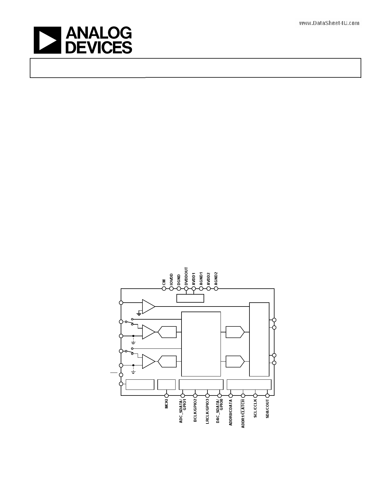
FUNCTIONAL BLOCK DIAGRAM
www.DataSheet4U.com
BEEP
LMIC/LMICN/
MICD1
LMICP
RMIC/RMICN/
MICD2
RMICP
PDN
MICBIAS
PGA
PGA
PGA
MICROPHONE
BIAS
REGULATOR
ADAU1381
LEFT
ADC
RIGHT
ADC
SOUND ENGINE
DECIMATION
FILTERS
WIND NOISE
NOTCH FILTER
EQUALIZER
DIGITAL VOLUME
CONTROL
AUTOMATIC LEVEL
CONTROL
LEFT
DAC
RIGHT
DAC
OUTPUT
MIXER
PLL
SERIAL DATA
INPUT/OUTPUT PORTS
I2C/SPI
CONTROL PORT
AOUTL
AOUTR
SPP
SPN
Figure 1.
Rev. 0
Information furnished by Analog Devices is believed to be accurate and reliable. However, no
responsibility is assumed by Analog Devices for its use, nor for any infringements of patents or other
rights of third parties that may result from its use. Specifications subject to change without notice. No
license is granted by implication or otherwise under any patent or patent rights of Analog Devices.
Trademarksandregisteredtrademarksarethepropertyoftheirrespectiveowners.
One Technology Way, P.O. Box 9106, Norwood, MA 02062-9106, U.S.A.
Tel: 781.329.4700
www.analog.com
Fax: 781.461.3113
©2009 Analog Devices, Inc. All rights reserved.
1 page 
Parameter
Left/Right Microphone PGA Gain
Range
Left/Right Microphone PGA Mute
Attenuation
Interchannel Gain Mismatch
Offset Error
Gain Error
Interchannel Isolation
Power Supply Rejection Ratio
DIFFERENTIAL MICROPHONE INPUT TO
ADC PATH
Full-Scale Input Voltage (0 dB)
Dynamic Range
With A-Weighted Filter (RMS)
No Filter (RMS)
Total Harmonic Distortion + Noise
Signal-to-Noise Ratio
With A-Weighted Filter (RMS)
No Filter (RMS)
Left/Right Microphone PGA Mute
Attenuation
Interchannel Gain Mismatch
www.DataOSfhfseeett4EUrr.ocor m
Gain Error
Interchannel Isolation
Common-Mode Rejection Ratio
BEEP TO LINE OUTPUT PATH
Full-Scale Input Voltage (0 dB)
Total Harmonic Distortion + Noise
Signal-to-Noise Ratio
With A-Weighted Filter (RMS)
No Filter (RMS)
Test Conditions/Comments
AVDD = 3.3 V
AVDD = 3.3 V; mute set by Register
0x400E, Bit 1, and Register 0x400F, Bit 1
AVDD = 3.3 V
AVDD = 3.3 V
AVDD = 3.3 V
AVDD = 3.3 V
CM capacitor = 10 μF
AVDD = 3.3 V, 100 mV p-p at 217 Hz
AVDD = 3.3 V, 100 mV p-p at 1 kHz
Min
0
Scales linearly with AVDD
AVDD = 1.8 V
AVDD = 3.3 V
−60 dB input
AVDD = 1.8 V
AVDD = 3.3 V
AVDD = 1.8 V
AVDD = 3.3 V
−3 dBFS
AVDD = 1.8 V
AVDD = 3.3 V
94
92
AVDD = 1.8 V
AVDD = 3.3 V
AVDD = 1.8 V
AVDD = 3.3 V
AVDD = 3.3 V; mute set by Register
0x400E, Bit 1, and Register 0x400F, Bit 1
AVDD = 3.3 V
AVDD = 3.3 V
AVDD = 3.3 V
AVDD = 3.3 V
AVDD = 3.3 V, 100 mV rms, 1 kHz
AVDD = 3.3 V, 100 mV rms, 20 kHz
Scales linearly with AVDD
AVDD = 1.8 V
AVDD = 3.3 V
−3 dBFS input, measured at AOUTL pin,
beep gain set to 0 dB
AVDD = 1.8 V
AVDD = 3.3 V
AVDD = 1.8 V
AVDD = 3.3 V
AVDD = 1.8 V
AVDD = 3.3 V
ADAU1381
Typ Max Unit
32 dB
−98 dB
50 mdB
0.25 mV
−1 %
−98 dB
−55 dB
−55 dB
AVDD/3.3
0.55 (1.56)
1.0 (2.83)
96
99.2
92
96.5
−84
−85
96
100
92
97
−98
50
0.25
−1
−85
−60
−45
AVDD/3.3
0.55 (1.56)
1.0 (2.83)
V rms
V rms (V p-p)
V rms (V p-p)
dB
dB
dB
dB
dB
dB
dB
dB
dB
dB
dB
mdB
mV
%
dB
dB
dB
V rms
V rms (V p-p)
V rms (V p-p)
−88 dB
−88 dB
99 dB
105 dB
96 dB
102 dB
Rev. 0| Page 5 of 84
5 Page 
ADAU1381
DIGITAL TIMING SPECIFICATIONS
−25°C < TA < +85°C, IOVDD = 1.62 V to 3.63 V, unless otherwise specified.
Table 7. Digital Timing
Parameter
MASTER CLOCK
tMP
Duty Cycle
SERIAL PORT
tBIL
tBIH
tLIS
tLIH
tSIS
tSIH
tSODM
SPI PORT
fCCLK,R
fCCLK,R
fCCLK,W
fCCLK,W
tCCPL
tCCPH
tCLS
tCLH
tCLPH
tCDS
tCDH
tCOD
www.DaI2tCaSPhOeReTt4U.com
fSCL
tSCLH
tSCLL
tSCS
tSCH
tDS
tSCR
tSCF
tSDR
tSDF
tBFT
DIGITAL MICROPHONE
tDCF
tDCR
tDDV
tDDH
Limit
tMIN
tMAX
50 90.9
30 70
10
10
5
5
5
5
70
5
10
25
25
10
10
10
5
10
5
5
70
40
400
0.6
1.3
0.6
0.6
100
300
300
300
300
0.6
10
10
22 30
0 12
Unit Description
ns Master clock (MCLK) period (that is, period of the signal input to MCKI).
%
ns BCLK pulse width low.
ns BCLK pulse width high.
ns LRCLK setup. Time to BCLK rising.
ns LRCLK hold. Time from BCLK rising.
ns DAC_SDATA setup. Time to BCLK rising.
ns DAC_SDATA hold. Time from BCLK rising.
ns ADC_SDATA delay. Time from BCLK falling in master mode.
MHz CCLK frequency, read operation, IOVDD = 1.8 V ± 10%.
MHz CCLK frequency, read operation, IOVDD = 3.3 V ± 10%.
MHz CCLK frequency, write operation, IOVDD = 1.8 V ± 10%.
MHz CCLK frequency, write operation, IOVDD = 3.3 V ± 10%.
ns CCLK pulse width low.
ns CCLK pulse width high.
ns CLATCH setup. Time to CCLK rising.
ns CLATCH hold. Time from CCLK rising.
ns CLATCH pulse width high.
ns CDATA setup. Time to CCLK rising.
ns CDATA hold. Time from CCLK rising.
COUT delay from CCLK edge to valid data, IOVDD = 1.8 V ± 10%.
ns COUT delay from CCLK edge to valid data, IOVDD = 3.3 V ± 10%.
kHz SCL frequency.
μs SCL high.
μs SCL low.
μs Setup time; relevant for repeated start condition.
μs Hold time. After this period, the first clock is generated.
ns Data setup time.
ns SCL rise time.
ns SCL fall time.
ns SDA rise time.
ns SDA fall time.
μs Bus-free time. Time between stop and start.
RL = 1 MΩ, CL = 14 pF.
ns Digital microphone clock fall time.
ns Digital microphone clock rise time.
ns Digital microphone delay time for valid data.
ns Digital microphone delay time for data three-stated.
Rev. 0| Page 11 of 84
11 Page | ||
| Páginas | Total 30 Páginas | |
| PDF Descargar | [ Datasheet ADAU1381.PDF ] | |
Hoja de datos destacado
| Número de pieza | Descripción | Fabricantes |
| ADAU1381 | Low Noise Stereo Codec | Analog Devices |
| ADAU1382 | Low Noise Stereo Codec | Analog Devices |
| Número de pieza | Descripción | Fabricantes |
| SLA6805M | High Voltage 3 phase Motor Driver IC. |
Sanken |
| SDC1742 | 12- and 14-Bit Hybrid Synchro / Resolver-to-Digital Converters. |
Analog Devices |
|
DataSheet.es es una pagina web que funciona como un repositorio de manuales o hoja de datos de muchos de los productos más populares, |
| DataSheet.es | 2020 | Privacy Policy | Contacto | Buscar |