|
|
PDF ICL7121 Data sheet ( Hoja de datos )
| Número de pieza | ICL7121 | |
| Descripción | 16-Bit Multiplying Microprocessor-Compatible D/A Converter | |
| Fabricantes | Intersil Corporation | |
| Logotipo |  |
|
Hay una vista previa y un enlace de descarga de ICL7121 (archivo pdf) en la parte inferior de esta página. Total 10 Páginas | ||
|
No Preview Available !
October 1997
®
ICL7121NOT
RECOMMENDED
FOR NEW DESIGNS
16-Bit Multiplying
Microprocessor-Compatible D/A Converter
Features
• 16-Bit Resolution
• Low Integral Linearity Error -0.003% FSR
• Monotonic to 16 Bits Over Full Military Temperature
Range (LM Grade)
• Microprocessor Compatible with Buffered Inputs
• Bipolar Application Requires No External Resistors
• Output Current Settling Time 3µs Max (1µs Typ)
• Low Linerarity and Gain Temperature Coefficients
• Low Power Dissipation (25mW)
• Full Four-Quadrant Multiplication
• Low Differential Nonlinearity Error at Bipolor Zero
Ordering Information
PART NUMBER
ICL7121JCJI
ICL7121JMJI
ICL7121KCJI
ICL7121KMJI
ICL7121LCJI
ICL7121LMJI
TEMP. RANGE
(oC)
PACKAGE
0 to 70
28 Ld CERDIP
-55 to 125 28 Ld CERDIP
0 to 70
28 Ld CERDIP
-55 to 125 28 Ld CERDIP
0 to 70
28 Ld CERDIP
-55 to 125 28 Ld CERDIP
Description
The ICL7121 achieves 0.003% linearity without laser
trimming by combining a four quadrant multiplying DAC
using thin film resistors with an on-chip PROM-controlled
correction circuit. Silicon-gate CMOS circuitry keeps the
power dissipation very low.
Microprocessor bus interfacing is eased using standard
memory WRITE cycle timing and control. The input buffer
register is loaded with the 16-bit input and directly controls
the output switches. The register is transparent if WR and
CS are held low.
The ICL7121 is designed and programmed for bipolar
operation. There is an offset resistor to the output which
should be connected to -VREF and an inverter on the MSB
line, giving the DAC a 2’s complement bipolar transfer
function. Two extra resistors are included on the chip to
facilitate the reference inversion, so that only an external op-
amp is needed.
www.DatPaSihneoetu4Ut.com
ICL7121
(OUTLINE DWG JI)
TOP VIEW
(LSB) D0 1
D1 2
D2 3
D3 4
D4 5
D5 6
D6 7
D7 8
D8 9
D9 10
D10 11
D11 12
D12 13
D13 14
28 CS
27 WR
26 V+
25 IOUT
24 AGNDS
23 AGNDF
22 DGND
21 RFB
20 ROFS
19 RINV
18 VREF
17 PROG
16 D15 (MSB)
15 D14
CAUTION: These devices are sensitive to electrostatic discharge; follow proper IC Handling Procedures.
1-888-INTERSIL or 321-724-7143 | Intersil (and design) is a registered trademark of Intersil Americas Inc.
Copyright © Intersil Americas Inc. 2002. All Rights Reserved
1
File Number 3112.1
1 page 
ICL7121
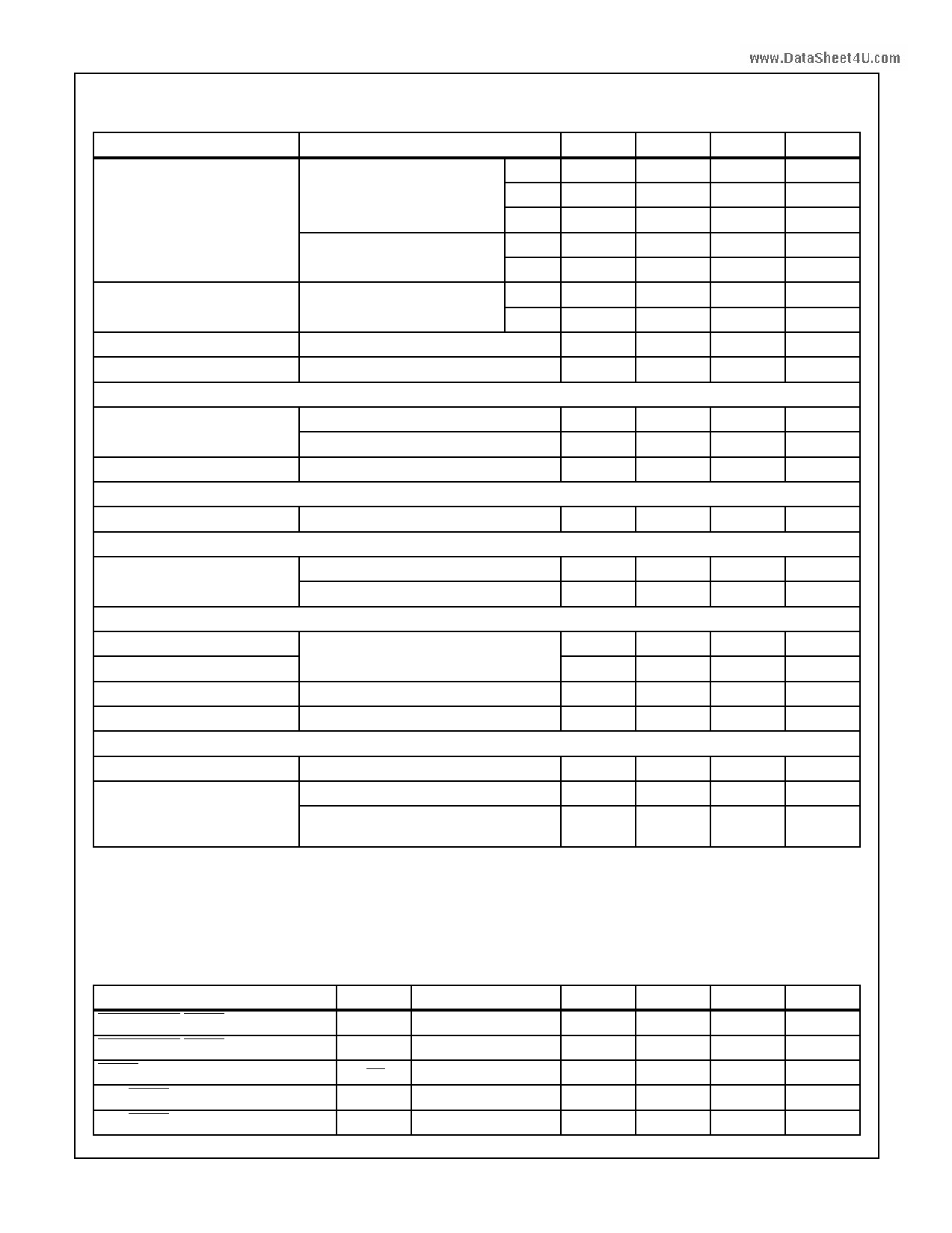
Electrical Specifications V+ = +5V, VREF = +5V, TA = 25oC, AGND = DGND, IOUT at Ground Potential,
Unless Otherwise Specified (Continued)
PARAMETER
Unadjusted Gain Error
TEST CONDITIONS
TA = 25oC
J
K
MIN
TYP
MAX
UNITS
-
±0.004
±0.012
%FSR
-
±0.003
±0.009
%FSR
L
-
±0.002
±0.006
%FSR
Operating Temperature Range
J
-
±0.002
+0.04
%FSR
Unadjusted Gain Error
Temperature Coefficient
(Note 4)
K, L -
J-
K, L -
±0.01
±1.0
±0.5
±0.02
±5.2
±2.0
%FSR
ppm/oC
ppm/oC
Unadjusted Output Offset
Output Offset Temperature Drift
DAC Register Outputs All LOW (Note 6)
Same Conditions as Above, (Note 4)
- ±4 ±15 mV
- - ±5 µV/oC
AC ACCURACY
Power Supply Rejection
∆V+ = 5V ±10%, TA = 25oC
Operating Temperature Range
-
±30
±100
ppm/C
-
±50
±150
ppm/C
Output Current Settling Time
To 1/2 LSB (Note 4)
- 1.8 3 µs
REFERENCE INPUT
Input Resistance
ANALOG OUTPUT
IOUT at Ground
3 4.2 6 kΩ
Output Capacitance
(IOUT Terminal)
DAC Register Outputs All Low
DAC Register Outputs All High
- 150 -
- 300 -
pF
pF
DIGITAL INPUTS
LOW State Threshold
Operating Temperature Range
- - 0.8 V
HIGH State Threshold
2.4 -
-V
Input Current
Inputs Between DGND to V+
-
±0.001
±1
µA
Input Capacitance
(Note 4)
- 15 - pF
www.DataPSOheWeEt4RU.ScUomPPLY
Supply Voltage Rnage *
Functional Operation (Note 5)
4.5 - 5.5 V
Supply Current
(Excluding Ladder Network)
TA = 25oC, Digital Inputs High or LOW
Operating Temperature Range Digital Inputs
HIGH or LOW
-
-
0.6 1.5 mA
1.0 2.5 mA
NOTES:
3. Military temperature range parts are also tested to stated limits at -55oC and 125oC.
4. Guaranteed by characterization but not tested on a production basis.
5. Guaranteed by PSRR test.
6. Refer to FIgure 1. Measured at output amplifier A1 (A1 having zero offset). VREF = +5V. Adjustable to zero with external potentiometer.
Switching Specifications V+ = 5V, TA = 25oC, See Timing Diagram
PARAMETER
SYMBOL TEST CONDITIONS
MIN
TYP
MAX
UNITS
CHIP SELECT-WRITE Set-Up Time
CHIP SELECT-WRITE Hold Time
WRITE Pulse Width Low
Data-WRITE Set-Up Time
Data-WRITE Hold Time
tCWs
tCWh
tWR
tDWs
tDWh
Note 4
Note 4
Note 4
Note 4
Note 4
0-
0-
200 -
200 -
0-
- ns
- ns
- ns
- ns
- ns
5
5 Page | ||
| Páginas | Total 10 Páginas | |
| PDF Descargar | [ Datasheet ICL7121.PDF ] | |
Hoja de datos destacado
| Número de pieza | Descripción | Fabricantes |
| ICL7121 | 16-Bit Multiplying Microprocessor-Compatible D/A Converter | Intersil Corporation |
| ICL7126 | Low Power/ 3 Digit A/D Converter | Maxim Integrated |
| ICL7126 | Single Chip A/D Converter | Intersil |
| ICL7129 | 41/2 Digit LCD/ Single-Chip A/D Converter | Intersil |
| Número de pieza | Descripción | Fabricantes |
| SLA6805M | High Voltage 3 phase Motor Driver IC. |
Sanken |
| SDC1742 | 12- and 14-Bit Hybrid Synchro / Resolver-to-Digital Converters. |
Analog Devices |
|
DataSheet.es es una pagina web que funciona como un repositorio de manuales o hoja de datos de muchos de los productos más populares, |
| DataSheet.es | 2020 | Privacy Policy | Contacto | Buscar |
