|
|
PDF S-T111 Data sheet ( Hoja de datos )
| Número de pieza | S-T111 | |
| Descripción | HIGH RIPPLE-REJECTION LOW DROPOUT CMOS VOLTAGE REGULATOR | |
| Fabricantes | Seiko Instruments | |
| Logotipo |  |
|
Hay una vista previa y un enlace de descarga de S-T111 (archivo pdf) en la parte inferior de esta página. Total 23 Páginas | ||
|
No Preview Available !
Rev.2.1_00
HIGH RIPPLE-REJECTION
LOW DROPOUT CMOS VOLTAGE REGULATOR
S-T111 Series
The S-T111 Series is a positive voltage regulator with
a low dropout voltage, high output voltage accuracy,
and low current consumption developed based on
CMOS technology.
A built-in low on-resistance transistor provides a low
dropout voltage and large output current, and a built-
in overcurrent protector prevents the load current
from exceeding the current capacitance of the output
transistor. An ON/OFF circuit ensures a long battery
life. Compared with the voltage regulators using the
conventional CMOS process, a larger variety of
capacitors are available, including small ceramic
capacitors. A small SOT-23-5 package realizes high-
density mounting.
Features
• Output voltage:
1.5 V to 5.5 V, selectable in 0.1 V steps.
• High-accuracy output voltage: ±1.0%
• Low dropout voltage:
190 mV typ. (3.0 V output product, IOUT = 100 mA)
• Low current consumption:
During operation: 50 μA typ., 90 μA max.
During shutdown: 0.1 μA typ., 1.0 μA max.
• High peak current capability:
150 mA output is possible (at VIN ≥ VOUT(S) + 1.0 V)*1
• Built-in ON/OFF circuit:
Ensures long battery life.
• Low ESR capacitor can be used: A ceramic capacitor of 0.1 μF or more can be used for the output
capacitor.
• High ripple rejection:
80 dB typ. (at 1.0 kHz)
• Built-in overcurrent protector: Overcurrent of output transistor can be restricted.
• Small package:
www.DataS•heLeet4aUd.-cformee products
SOT-23-5
*1. Attention should be paid to the power dissipation of the package when the output current is large.
Applications
• Power supply for battery-powered devices
• Power supply for personal communication devices
• Power supply for home electric/electronic appliances
• Power supply for cellular phones
Package
Package Name
SOT-23-5
Package
MP005-A
Drawing Code
Tape
MP005-A
Reel
MP005-A
Seiko Instruments Inc.
1
1 page 
HIGH RIPPLE-REJECTION LOW DROPOUT CMOS VOLTAGE REGULATOR
Rev.2.1_00
S-T111 Series
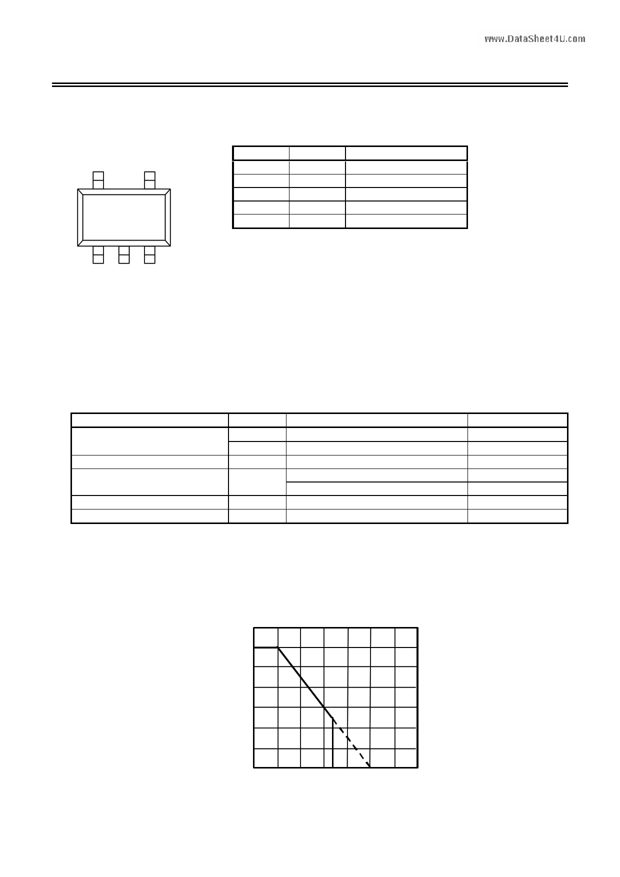
Pin Configuration
SOT-23-5
Top view
54
Table 2
Pin No. Symbol
Description
1 ON/OFF
Shutdown pin
2 VSS
3 NC*1
GND pin
No connection
4
VOUT
Output voltage pin
5 VIN Input voltage pin
*1. The NC pin is electrically open.
The NC pin can be connected to VIN or VSS.
123
Figure 2
Absolute Maximum Ratings
Table 3
(Ta = 25°C unless otherwise specified)
Item
Symbol
Absolute Maximum Rating
Unit
Input voltage
Output voltage
Power dissipation
VIN
VON/OFF
VOUT
PD
VSS − 0.3 to VSS + 7
VSS − 0.3 to VIN + 0.3
VSS − 0.3 to VIN + 0.3
300 (When not mounted on board)
600*1
V
V
V
mW
mW
Operating ambient temperature
Storage temperature
www.DataS*h1e.et4WUh.ceomn mounted on board
Topr
Tstg
−40 to +85
−40 to +125
°C
°C
[Mounted board]
(1) Board size : 114.3 mm × 76.2 mm × t1.6 mm
(2) Board name : JEDEC STANDARD51-7
Caution The absolute maximum ratings are rated values exceeding which the product could suffer
physical damage. These values must therefore not be exceeded under any conditions.
700
600
500
400
300
200
100
0
0 50 100 150
Ambient Temperature (Ta) [°C]
Figure 3 Power Dissipation of Package (When Mounted on Board)
Seiko Instruments Inc.
5
5 Page 
HIGH RIPPLE-REJECTION LOW DROPOUT CMOS VOLTAGE REGULATOR
Rev.2.1_00
S-T111 Series
Operation
1. Basic operation
Figure 11 shows the block diagram of the S-T111 Series.
The error amplifier compares the reference voltage (Vref) with Vfb, which is the output voltage resistance-
divided by feedback resistors Rs and Rf. It supplies the output transistor with the gate voltage necessary
to ensure a certain output voltage free of any fluctuations of input voltage and temperature.
VIN
Current
supply
Vref
Error
amplifier
−
+
Reference voltage
circuit
*1
Rf
Vfb
Rs
VOUT
VSS
*1. Parasitic diode
Figure 11
2. Output transistor
The S-T111 Series uses a low on-resistance P-channel MOS FET as the output transistor.
Be sure that VOUT does not exceed VIN + 0.3 V to prevent the voltage regulator from being damaged due
to inverse current flowing from the VOUT pin through a parasitic diode to the VIN pin.
www.DataSheet4U.com
Seiko Instruments Inc.
11
11 Page | ||
| Páginas | Total 23 Páginas | |
| PDF Descargar | [ Datasheet S-T111.PDF ] | |
Hoja de datos destacado
| Número de pieza | Descripción | Fabricantes |
| S-T111 | HIGH RIPPLE-REJECTION LOW DROPOUT CMOS VOLTAGE REGULATOR | Seiko Instruments |
| Número de pieza | Descripción | Fabricantes |
| SLA6805M | High Voltage 3 phase Motor Driver IC. |
Sanken |
| SDC1742 | 12- and 14-Bit Hybrid Synchro / Resolver-to-Digital Converters. |
Analog Devices |
|
DataSheet.es es una pagina web que funciona como un repositorio de manuales o hoja de datos de muchos de los productos más populares, |
| DataSheet.es | 2020 | Privacy Policy | Contacto | Buscar |
