|
|
|
PDF XR17V352 Data sheet ( Hoja de datos )
| Número de pieza | XR17V352 | |
| Descripción | HIGH PERFORMANCE DUAL PCI EXPRESS UART | |
| Fabricantes | Exar Corporation | |
| Logotipo | ||
Hay una vista previa y un enlace de descarga de XR17V352 (archivo pdf) en la parte inferior de esta página. Total 30 Páginas | ||
|
No Preview Available !
PRELIMINARY
XR17V352
HIGH PERFORMANCE DUAL PCI EXPRESS UART
JULY 2009
REV. P1.0.1
GENERAL DESCRIPTION
The XR17V3521 (V352) is a single chip 2-channel
PCI Express (PCIe) UART (Universal Asynchronous
Receiver and Transmitter), optimized for higher
performance and lower power. The V352 serves as a
single lane PCIe bridge to 2 indepedent enhanced
16550 compatible UARTs. The V352 is compliant to
PCIe 2.0 Gen 1 (2.5GT/s).
In addition to the UART channels, the V352 has 16
multi-purpose I/Os (MPIOs), a 16-bit general purpose
counter/timer and a global interrupt status register to
optimize interrupt servicing.
Each UART of the V352 has many enhanced
features such as the 256-bytes TX and RX FIFOs,
programmable Fractional Baud Rate Generator,
Automatic Hardware or Software Flow Control, Auto
RS-485 Half-Duplex Direction Control, programmable
TX and RX FIFO Trigger Levels, TX and RX FIFO
Level Counters, infrared mode, and data rates up to
25Mbps. The V352 is available in a 113-pin STBGA
package (9 x 9 mm).
NOTE 1: Covered by U.S. Patents #5,649,122, #6,754,839,
#6,865,626 and #6,947,999
APPLICATIONS
• Next generation Point-of-Sale Systems
• Remote Access Servers
• Storage Network Management
• Factory Automation and Process Control
www.DataS•heMet4uUlt.ic-pomort RS-232/RS-422/RS-485 Cards
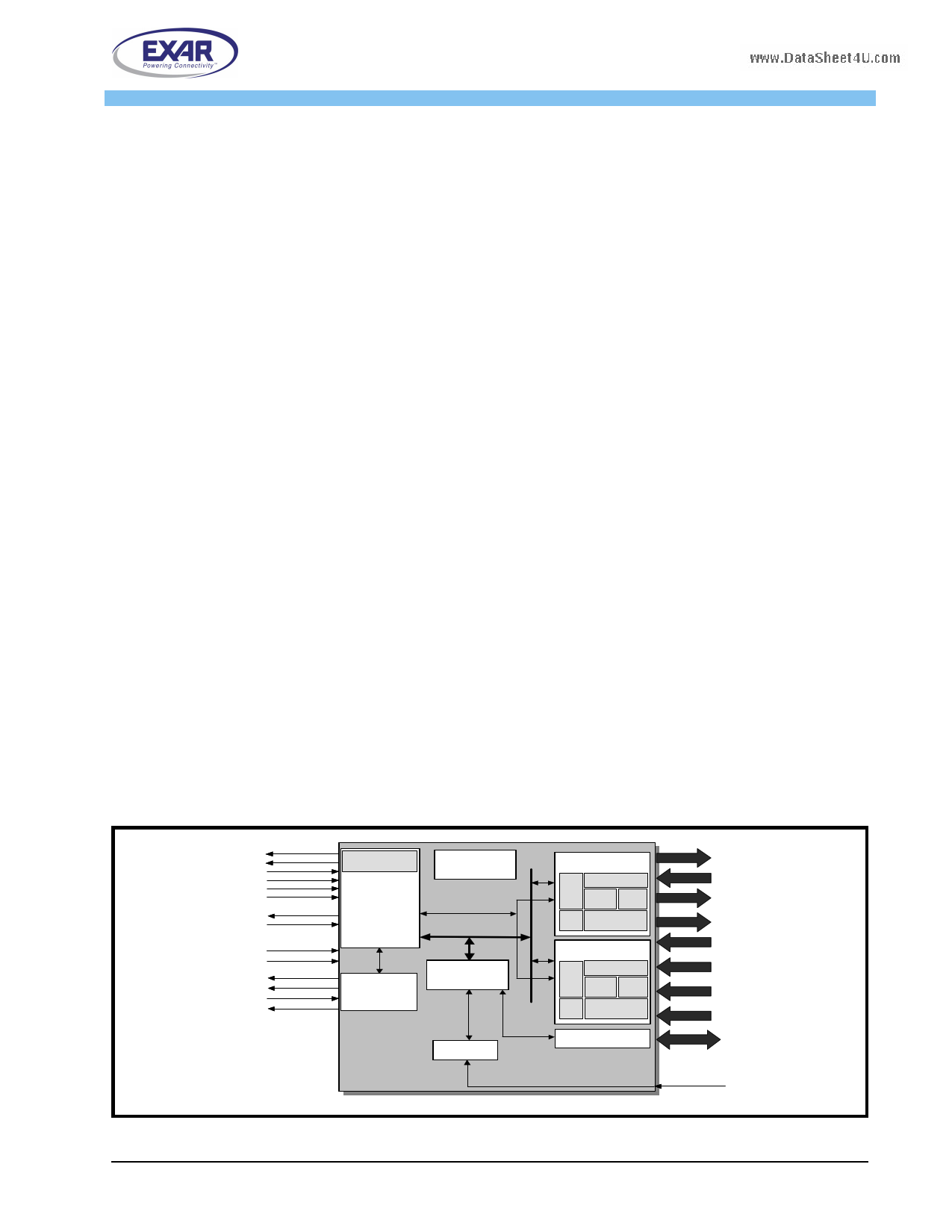
FIGURE 1. BLOCK DIAGRAM OF THE XR17V352
FEATURES
• Single 3.3V power supply
• Internal buck regulator for 1.2V core
• PCIe 2.0 Gen 1 compliant
• x1 Link, dual simplex, 2.5Gbps in each direction
• EEPROM interface for configuration
• Data read/write burst operation
• Global interrupt status register for both UARTs
• Up to 25 Mbps serial data rate
• 16 multi-purpose inputs/outputs (MPIOs)
• 16-bit general purpose timer/counter
• Sleep mode with wake-up Indicator
• Two independent UART channels controlled with
■ 16550 compatible register Set
■ 256-byte TX and RX FIFOs
■ Programmable TX and RX Trigger Levels
■ TX/RX FIFO Level Counters
■ Fractional baud rate generator
■ Automatic RTS/CTS or DTR/DSR hardware
flow control with programmable hysteresis
■ Automatic Xon/Xoff software flow control
■ RS-485 half duplex direction control output
with programmable turn-around delay
■ Multi-drop with Auto Address Detection
■ Infrared (IrDA 1.1) data encoder/decoder
• Software compatible to XR17C15x, XR17D15x,
XR17V25x PCI UARTs
TX+
TX-
RX+
RX-
CLK+
CLK-
CLKREQ#
RST#
EN485#
E N IR #
EECK
EEDI
EEDO
EECS
C o n fig u ratio n
Space
R eg isters
B uck R egulator
PInCtPIeCLr foIaeccael
Bus
In te rfa c e
C o n fig u ratio n
EREeSPgpiRascOt eeMr s
In te rfa c e
125 M H z C lo ck
G lobal
C onfiguration
R egisters
1166-- b it
TTimimeer /rC/Coouunnteter r
UUAARRTTCChhaannnneel l00
64- b yte TX FIFO
U A R T 256-b yte T X F IF O
URAeRg Ts
R eg s
BRG
TX & RX
TX & RX
64- byte
IR
EE NNIRDD EE CC
REXNFDIEF OC
B R G 256-b yte R X F IF O
UART Channel 2
UART Channel 1
256-b yte TX FIFO
UART
Regs
UA
TX
RT
&
C
RX
ha
n
IR
EnNeDl E5
C
B RUGA R2 5T6 -Cb yhtae nRnX eFlIF6O
M u lti-p u rp o se
In p u t s- /O u tp u t s
In p u ts/O u tp u ts
C rystal O sc/B uffer
TT XX [[ 17 :: 00 ]]
R X [1:0]
R X [7:0]
R TS#[1:0]
D T R #[1:0]
C T S #[1:0]
D S R #[1:0]
D C D #[1:0]
R I#[1:0]
M P IO [15:0]
TM RCK
Exar Corporation 48720 Kato Road, Fremont CA, 94538 • (510) 668-7000 • FAX (510) 668-7017 • www.exar.com
1 page 
REV. P1.0.1
PIN DESCRIPTIONS
NAME
EEDI
PIN #
J8
EEDO
L9
JTAG SIGNALS
TRESET
L6
TCK
K6
TMS
J6
TDI L7
TDO
K7
BUCK REGULATOR SIGNALS
ENABLE
C10
LX A9
LX A10
FB C7
PWRGD
D9
ANCILLARY SIGNALS
RESET#
J5
TMRCK
A6
www.DataSheet4EUN.co4m85#
C6
ENIR#
B6
TEST0
TEST1
TEST2
TEST3
TEST4#
TEST5
VCC33
VCC33A
VCC33P
D2
B7
A7
D10
E10
E9
D5, E8, H7
H3
B9, C9
PRELIMINARY
XR17V352
HIGH PERFORMANCE DUAL PCI EXPRESS UART
TYPE
DESCRIPTION
O Write data to EEPROM device. It is manually accessible thru the Configura-
tion Register REGB.
I Read data from EEPROM device. It is manually accessible thru the Configu-
ration Register REGB.
I JTAG Test Reset
I JTAG Test Clock
I JTAG Test Mode Select
I JTAG Data Input
O JTAG Data Output
I Connect to VCC to enable buck regulator. Connect to GND to disable buck
regulator.
O Connect these two signals together to external 4.7uH inductor.
O
I Connect this signal to other end of external 4.7uH inductor. 47uF capacitor to
GND is also required on this pin.
O Indicates that 1.2V core has been powered up.
I System reset (active low). In normal operation, this signal should be HIGH.
I 16-bit timer/counter external clock input.
I Auto RS-485 mode enable (active low). This pin is sampled during power up,
following a hardware reset (RST#) or soft reset (register RESET). It can be
used to start up both UARTs in the Auto RS-485 Half-Duplex Direction control
mode. The sampled logic state is transferred to FCTR bit-5 in the UART
channel.
I Infrared mode enable (active low). This pin is sampled during power up, fol-
lowing a hardware reset (RST#) or soft-reset (register RESET). It can be
used to start up both UARTs in the infrared mode. The sampled logic state is
transferred to MCR bit-6 in the UART.
I Factory Test Modes. For normal operation, connect to GND.
I
I
I
I Factory Test Mode 4. For normal operation, connect to VCC.
I/O Factory Test I/O. For normal operation, connect to pull-down resistor.
Pwr 3.3V I/O power supply.
Pwr 3.3V analog PHY power supply. A ferrite bead is recommended on this pin.
Pwr 3.3V power supply voltage for output stage of buck regulator.
5
5 Page 
REV. P1.0.1
ADDRESS
OFFSET
BITS
0x80 31:16
15:8
7:0
0x84 31:16
15:8
7:0
0x88 31:16
15:8
7:0
0x8C 31:24
23:22
21:18
17:15
14:12
11:10
9:4
3:0
0x90 31:21
www.DataSheet4U.com 20
19
18
17:15
14:10
9:4
3:0
0x94 31:0
0x98-0xAF 31:0
0xB0 31:0
0xB4-0xFF 31:0
0x100 31:0
PRELIMINARY
XR17V352
HIGH PERFORMANCE DUAL PCI EXPRESS UART
TABLE 1: PCI LOCAL BUS CONFIGURATION SPACE REGISTERS
TYPE
DESCRIPTION
RESET VALUE
(HEX OR BINARY)
RO PCI Express 2.0 capable endpoint, Interrupt Message Number 1
0x0202
RO Next Capability Pointer
0x00
RO PCI Express Capability ID
0x10
RO Not implemented or not applicable (return zeros)
0x0000
RO Role-Based Error Reporting
0x80
RO 256 bytes max payload size
0x01
RW Not implemented or not applicable (return zeros)
0x0000
RW 512 bytes max read request, Enable No Snoop
0x28
RW 256 bytes max TLP payload size
0x10
RO Port Number
0x01
RO Not implemented or not applicable (return zeros)
00b
RO Not implemented or not applicable (return zeros)
0000b
RO L1 Exit Latency < 1 us
000b
RO L0s Exit Latency < 64 ns
000b
RO Active State Power Management (ASPM) Support
L0s and L1 Supported
11b
RO x1 max Link Width
000001b
RO 2.5GT/s Link speed supported
0001b
RO Not implemented or not applicable (return zeros)
00000000000b
RO Data Link Layer Active Reporting capable
1b
RO Surprise Down Error Reporting not supported
0b
RO Reference clock must not be removed.
0b
RO L1 Exit Latency - 2 us to less than 4 us
010b
RO Not implemented or not applicable (return zeros)
00000b
RO x1 negotiated Link Width
000001b
RO Current Link Speed is 2.5GT/s
0001b
RO PCIe Capability Offset 0x14 - Slot Capabilities Register
0x00040000
RO Not implemented or not applicable (return zeros)
0x00000000
RO PCIe Capability Offset 0x30 - Link Status2/Control2
0x00010001
RO Not implemented or not applicable (return zeros)
0x00000000
RO VC Resource Capability Register
0x00010002
11
11 Page | ||
| Páginas | Total 30 Páginas | |
| PDF Descargar | [ Datasheet XR17V352.PDF ] | |
Hoja de datos destacado
| Número de pieza | Descripción | Fabricantes |
| XR17V352 | HIGH PERFORMANCE DUAL PCI EXPRESS UART | Exar Corporation |
| XR17V354 | HIGH PERFORMANCE QUAD PCI-EXPRESS UART | Exar Corporation |
| XR17V358 | HIGH PERFORMANCE OCTAL PCI EXPRESS UART | Exar Corporation |
| Número de pieza | Descripción | Fabricantes |
| SLA6805M | High Voltage 3 phase Motor Driver IC. |
Sanken |
| SDC1742 | 12- and 14-Bit Hybrid Synchro / Resolver-to-Digital Converters. |
Analog Devices |
|
DataSheet.es es una pagina web que funciona como un repositorio de manuales o hoja de datos de muchos de los productos más populares, |
| DataSheet.es | 2020 | Privacy Policy | Contacto | Buscar |