|
|
|
PDF ADG1607 Data sheet ( Hoja de datos )
| Número de pieza | ADG1607 | |
| Descripción | (ADG1606 / ADG1607) Multiplexers | |
| Fabricantes | Analog Devices | |
| Logotipo | ||
Hay una vista previa y un enlace de descarga de ADG1607 (archivo pdf) en la parte inferior de esta página. Total 24 Páginas | ||
|
No Preview Available !
4.5 Ω RON, 16-Channel, Differential 8-Channel,
±5 V,+12 V,+5 V, and +3.3 V Multiplexers
ADG1606/ADG1607
FEATURES
4.5 Ω typical on resistance
1.1 Ω on resistance flatness
±3.3 V to ±8 V dual supply operation
3.3 V to 16 V single supply operation
No VL supply required
3 V logic-compatible inputs
Rail-to-rail operation
Up to 378 mA of continuous current per channel
28-lead TSSOP and 32-lead, 5 mm × 5 mm LFCSP_VQ
APPLICATIONS
Communication systems
Medical systems
Audio signal routing
Video signal routing
Automatic test equipment
Data acquisition systems
Battery-powered systems
Sample-and-hold systems
Relay replacements
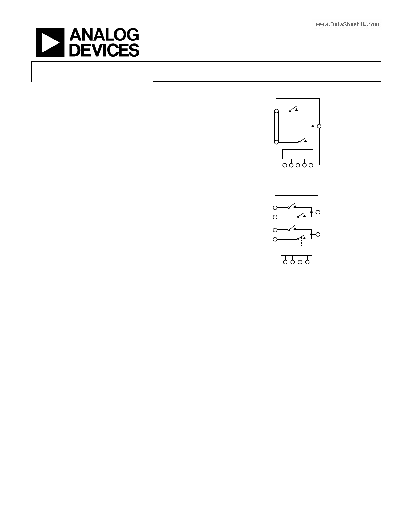
FUNCTIONAL BLOCK DIAGRAMS
ADG1606
S1
D
S16
1-OF-16
DECODER
A0 A1 A2 A3 EN
Figure 1.
ADG1607
S1A
DA
S8A
S1B
DB
S8B
1-OF-8
DECODER
A0 A1 A2 EN
Figure 2.
GENERAL DESCRIPTION
The ADG1606 and ADG1607 are monolithic iCMOS® analog
www.DamtauSlthipeleetx4eUr.scocommprising of 16 single channels and eight
differential channels, respectively. The ADG1606 switches one of
16 inputs to a common output, as determined by the 4-bit
binary address lines (A0, A1, A2, and A3). The ADG1607
switches one of eight differential inputs to a common differential
output, as determined by the 3-bit binary address lines (A0, A1,
and A2). An EN input on both devices enables or disables the
device. When disabled, all channels switch off. When enabled,
each channel conducts equally well in both directions and has an
input signal range that extends to the supplies.
The ultralow on resistance and on-resistance flatness of these
switches make them ideal solutions for data acquisition and
gain switching applications where low distortion is critical.
iCMOS® construction ensures ultralow power dissipation,
making the parts ideally suited for portable and battery-
powered instruments.
PRODUCT HIGHLIGHTS
1. 7.5 Ω maximum on resistance over temperature.
2. Minimum distortion: THD + N = 0.04%
3. 3 V logic-compatible digital inputs: VINH = 2.0 V, VINL = 0.8 V.
4. No VL logic power supply required.
Rev. 0
Information furnished by Analog Devices is believed to be accurate and reliable. However, no
responsibility is assumed by Analog Devices for its use, nor for any infringements of patents or other
rights of third parties that may result from its use. Specifications subject to change without notice. No
license is granted by implication or otherwise under any patent or patent rights of Analog Devices.
Trademarksandregisteredtrademarksarethepropertyoftheirrespectiveowners.
One Technology Way, P.O. Box 9106, Norwood, MA 02062-9106, U.S.A.
Tel: 781.329.4700
www.analog.com
Fax: 781.461.3113
©2009 Analog Devices, Inc. All rights reserved.
1 page 
ADG1606/ADG1607
5 V SINGLE SUPPLY
VDD = 5 V ± 10%, VSS = 0 V, GND = 0 V, unless otherwise noted.
Table 3.
Parameter
ANALOG SWITCH
Analog Signal Range
On Resistance (RON)
On Resistance Match Between Channels (∆RON)
On Resistance Flatness (RFLAT(ON))
LEAKAGE CURRENTS
Source Off Leakage, IS (Off)
Drain Off Leakage, ID (Off)
ADG1606
Channel On Leakage, ID, IS (On)
DIGITAL INPUTS
Input High Voltage, VINH
Input Low Voltage, VINL
Input Current, IINL or IINH
25°C
−40°C to
+85°C
8.5
9.5 11.5
0.3
0.8 1.1
1.8
2.4 2.7
±0.01
±0.15
±0.02
±0.2
±0.05
±0.3
±0.5
±3
±3
±0.003
Digital Input Capacitance, CIN
DYNAMIC CHARACTERISTICS1
Transition Time, tTRANSITION
tON (EN)
tOFF (EN)
Break-Before-Make Time Delay, tBBM
www.DataCShhaergeet4InUj.eccotimon
Off Isolation
Channel-to-Channel Crosstalk
Total Harmonic Distortion + Noise (THD + N)
4
220
280 324
160
202 221
154
197 232
45
12
−62
−62
0.35
−3 dB Bandwidth
ADG1606
ADG1607
CS (Off)
CD (Off)
ADG1606
ADG1607
CD, CS (On)
ADG1606
ADG1607
POWER REQUIREMENTS
IDD
19
34
20
270
137
300
160
0.001
VDD
1 Guaranteed by design, not subject to production test.
−40°C to
+125°C Unit
0 V to VDD
12.5
1.2
3
V
Ω typ
Ω max
Ω typ
Ω max
Ω typ
Ω max
nA typ
±3 nA max
nA typ
±25 nA max
nA typ
±25 nA max
2.0 V min
0.8 V max
μA typ
±0.1 μA max
pF typ
ns typ
360 ns max
ns typ
234 ns max
ns typ
259 ns max
ns typ
15 ns min
pC typ
dB typ
dB typ
% typ
1.0
3.3/16
MHz typ
MHz typ
pF typ
pF typ
pF typ
pF typ
pF typ
μA typ
μA max
V min/max
Test Conditions/Comments
VS = 0 V to 4.5 V, IS = −10 mA; see Figure 26
VDD = 4.5 V, VSS = 0 V
VS = 0 V to 4.5 V, IS = −10 mA
VS = 0 V to 4.5 V, IS = −10 mA
VDD = 5.5 V, VSS = 0 V
VS = 1 V/4.5 V, VD = 4.5 V/1 V; see Figure 27
VS = 1 V/4.5 V, VD = 4.5 V/1 V; see Figure 27
VS = VD = 1 V or 4.5 V; see Figure 28
VIN = VGND or VDD
RL = 300 Ω, CL = 35 pF
VS = 2.5 V; see Figure 29
RL = 300 Ω, CL = 35 pF
VS = 2.5 V; see Figure 31
RL = 300 Ω, CL = 35 pF
VS = 2.5 V; see Figure 31
RL = 300 Ω, CL = 35 pF
VS1 = VS2 = 2.5 V; see Figure 30
VS = 2.5 V, RS = 0 Ω, CL = 1 nF; see Figure 32
RL = 50 Ω, CL = 5 pF, f = 1 MHz; see Figure 33
RL = 50 Ω, CL = 5 pF, f = 1 MHz; see Figure 35
RL = 110 Ω, f = 20 Hz to 20 kHz, VS = 3.5 V p-p; see
Figure 36
RL = 50 Ω, CL = 5 pF; see Figure 34
VS = 2.5 V, f = 1 MHz
VS = 2.5 V, f = 1 MHz
VS = 2.5 V, f = 1 MHz
VS = 2.5 V, f = 1 MHz
VS = 2.5 V, f = 1 MHz
VDD = 5.5 V
Digital inputs = 0 V or VDD
Rev. 0 | Page 5 of 24
5 Page 
ADG1606/ADG1607
VDD 1
DB 2
28 DA
27 VSS
NC 3
26 S8A
S8B 4
25 S7A
S7B 5
S6B 6
S5B 7
ADG1607
TOP VIEW
(Not to Scale)
24 S6A
23 S5A
22 S4A
S4B 8
21 S3A
S3B 9
20 S2A
S2B 10
19 S1A
S1B 11
18 EN
GND 12
17 A0
NC 13
16 A1
NC 14
15 A2
NC = NO CONNECT
Figure 5. ADG1607 TSSOP Pin Configuration
S8B 1
S7B 2
S6B 3
S5B 4
S4B 5
S3B 6
S2B 7
S1B 8
PIN 1
INDICATOR
ADG1607
TOP VIEW
(Not to Scale)
24 S8A
23 S7A
22 S6A
21 S5A
20 S4A
19 S3A
18 S2A
17 S1A
NOTES
1. NC = NO CONNECT.
2. EXPOSED PAD TIED TO SUBSTRATE, VSS.
Figure 6. ADG1607 LFCSP_VQ Pin Configuration
Table 11. ADG1607 Pin Function Descriptions
Pin No.
TSSOP
LFCSP_VQ Mnemonic Description
1 29 VDD Most Positive Power Supply Potential.
2 31 DB Drain Terminal B. This pin can be an input or an output.
3, 13, 14
11, 12, 13, 26, NC
28, 30, 32
No Connect.
41
S8B Source Terminal 8B. This pin can be an input or an output.
52
S7B Source Terminal 7B. This pin can be an input or an output.
63
S6B Source Terminal 6B. This pin can be an input or an output.
74
S5B Source Terminal 5B. This pin can be an input or an output.
85
S4B Source Terminal 4B. This pin can be an input or an output.
96
S3B Source Terminal 3B. This pin can be an input or an output.
10 7
S2B Source Terminal 2B. This pin can be an input or an output.
11 8
S1B Source Terminal 1B. This pin can be an input or an output.
12 9
GND Ground (0 V) Reference.
15 10 A2 Logic Control Input.
www.Da1t6aSheet4U.com14 A1 Logic Control Input.
17 15 A0 Logic Control Input.
18 16 EN Active High Digital Input. When this pin is low, the device is disabled and all switches are
turned off. When this pin is high, the Ax logic inputs determine which switch is turned on.
19 17
S1A Source Terminal 1A. This pin can be an input or an output.
20 18
S2A Source Terminal 2A. This pin can be an input or an output.
21 19
S3A Source Terminal 3A. This pin can be an input or an output.
22 20
S4A Source Terminal 4A. This pin can be an input or an output.
23 21
S5A Source Terminal 5A. This pin can be an input or an output.
24 22
S6A Source Terminal 6A. This pin can be an input or an output.
25 23
S7A Source Terminal 7A. This pin can be an input or an output.
26 24
S8A Source Terminal 8A. This pin can be an input or an output.
27 25 VSS Most Negative Power Supply Potential. In single-supply applications, this pin can be
connected to ground.
28 27 DA Drain Terminal A. This pin can be an input or an output.
EPAD
Exposed Pad The exposed pad is connected internally. For increased reliability of the solder joints and
maximum thermal capability, it is recommended that the pad be soldered to the substrate, VSS.
Rev. 0 | Page 11 of 24
11 Page | ||
| Páginas | Total 24 Páginas | |
| PDF Descargar | [ Datasheet ADG1607.PDF ] | |
Hoja de datos destacado
| Número de pieza | Descripción | Fabricantes |
| ADG1604 | Resistance | Analog Devices |
| ADG1606 | (ADG1606 / ADG1607) Multiplexers | Analog Devices |
| ADG1607 | (ADG1606 / ADG1607) Multiplexers | Analog Devices |
| ADG1608 | (ADG1608 / ADG1609) Multiplexer | Analog Devices |
| Número de pieza | Descripción | Fabricantes |
| SLA6805M | High Voltage 3 phase Motor Driver IC. |
Sanken |
| SDC1742 | 12- and 14-Bit Hybrid Synchro / Resolver-to-Digital Converters. |
Analog Devices |
|
DataSheet.es es una pagina web que funciona como un repositorio de manuales o hoja de datos de muchos de los productos más populares, |
| DataSheet.es | 2020 | Privacy Policy | Contacto | Buscar |