|
|
PDF W25P10 Data sheet ( Hoja de datos )
| Número de pieza | W25P10 | |
| Descripción | (W25P10 - W25P40) SERIAL FLASH MEMORY | |
| Fabricantes | Winbond | |
| Logotipo |  |
|
Hay una vista previa y un enlace de descarga de W25P10 (archivo pdf) en la parte inferior de esta página. Total 30 Páginas | ||
|
No Preview Available !
W25P10, W25P20 AND W25P40
1M-BIT, 2M-BIT AND 4M-BIT
SERIAL FLASH MEMORY WITH 40MHZ SPI
Formally NexFlash NX25P10, NX25P20 and NX25P40
The Winbond W25P10/20/40 are fully compatible with the previous NexFlash
NX25P10/20/40 Serial Flash memories.
www.DataSheet4U.com
Publication Release Date: November 28, 2005
- 1 - Revision M
1 page 
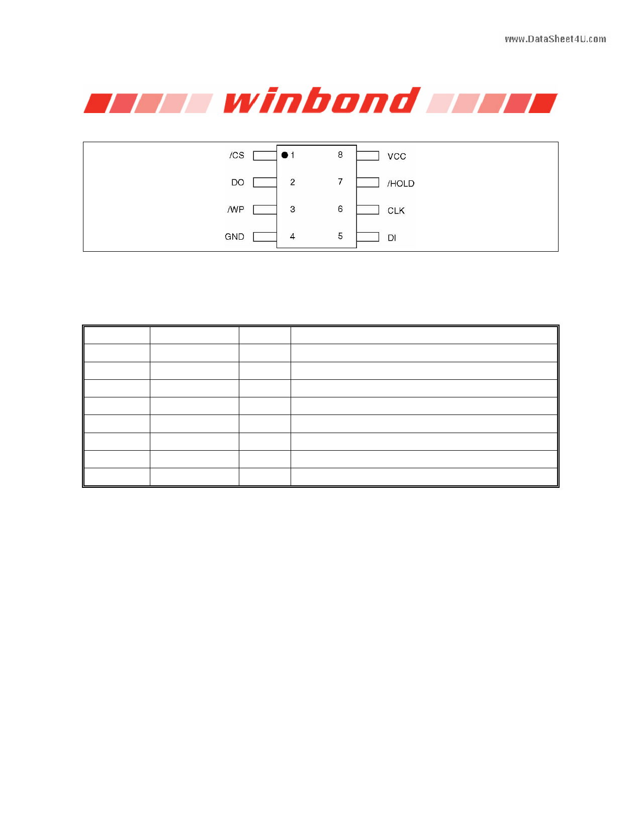
3. PIN CONFIGURATION
W25P10, W25P20 AND W25P40
Figure 1. W25P10, W25P20 and W25P40 Pin Assignments, 8-pin SOIC 150-mil
4. PIN DESCRIPTION
PIN NO.
1
2
3
4
5
6
7
8
PIN NAME
/CS
DO
/WP
GND
DI
CLK
/HOLD
VCC
I/O FUNCTION
I Chip Select Input
O Data Output
I Write Protect Input
Ground
I Data Input
I Serial Clock Input
I Hold Input
Power Supply
www.DataSheet4U.com
4.1 Package Types
The standard package for the W25P10/20/40 is an 8-pin plastic SOIC with 150-mil body (Winbond
package code SN) (NexFlash package code N). It also allows a package migration path to higher
density Serial Flash devices. The pinout for the package is shown in Figure 1. Package diagrams and
dimensions are illustrated at the end of this data sheet. Optional 8-contact MLP packages may be
available. Please contact Winbond for further MLP package information.
4.2 Chip Select (/CS)
The SPI Chip Select (/CS pin enables and disables device operation. When /CS is high the device is
deselected and the Serial Data Output (DO) pin is at high impedance. When deselected, the devices
power consumption will be at standby levels unless an internal erase, program or status register cycle
is in progress. When /CS is brought low the device will be selected, power consumption will increase
to active levels and instructions can be written to and data read from the device. After power-up, /CS
must transition from high to low before a new instruction will be accepted. The /CS input must track
Publication Release Date: November 28, 2005
- 5 - Revision M
5 Page 
W25P10, W25P20 AND W25P40
7.1.6 Status Register Memory Protection
STATUS REGISTER(1)
W25P40 (4M-BIT) MEMORY PROTECTION
BP2 BP1 BP0 SECTOR(S)
ADDRESSES
00
0
NONE
NONE
00
1
7 070000h - 07FFFFh
01
0
6 and 7
060000h - 07FFFFh
01
1
4 thru 7
040000h - 07FFFFh
1x
x
ALL 000000h - 07FFFFh
DENSITY (KB)
NONE
512K-bit
1M-bit
2M-bit
4M-bit
PORTION
NONE
Upper 1/8
Upper 1/4
Upper 1/2
ALL
STATUS REGISTER(1)
BP2 BP1
x0
x0
x1
x1
BP0
0
1
0
1
SECTOR(S)
NONE
3
2 and 3
ALL
W25P20 (2M-BIT) MEMORY PROTECTION
ADDRESSES
NONE
030000h - 03FFFFh
020000h - 03FFFFh
000000h - 03FFFFh
DENSITY (KB)
NONE
512K-bit
1M-bit
2M-bit
PORTION
NONE
Upper 1/4
Upper 1/2
ALL
STATUS REGISTER(1)
BP2 BP1
x0
x1
x1
BP0
x
0
1
SECTOR(S)
NONE
NONE
ALL
W25P10 (1M-BIT) MEMORY PROTECTION
ADDRESSES
NONE
NONE
000000h - 01FFFFh
DENSITY (KB)
NONE
NONE
1M-bit
Note:
1. x = don’t care
PORTION
NONE
NONE
ALL
www.DataShe7et.42U.comINSTRUCTIONS
The instruction set of the W25P10/20/40 consists of twelve basic instructions that are fully controlled
through the SPI bus (see Instruction Set table). Instructions are initiated with the falling edge of Chip
Select (/CS). The first byte of data clocked into the DI input provides the instruction code. Data on the
DI input is sampled on the rising edge of clock with most significant bit (MSB) first.
Instructions vary in length from a single byte to several bytes and may be followed by address bytes,
data bytes, dummy bytes (don’t care), and in some cases, a combination. Instructions are completed
with the rising edge of edge /CS. Clock relative timing diagrams for each instruction are included in
figures 4 through 16. All read instructions can be completed after any clocked bit. However, all
instructions that Write, Program or Erase must complete on a byte boundary (/CS driven high after a
full 8-bits have been clocked) otherwise the instruction will be terminated. This feature further protects
the device from inadvertent writes. Additionally, while the memory is being programmed or erased, or
when the Status Register is being written, all instructions except for Read Status Register will be
ignored until the program or erase cycle has completed.
Publication Release Date: November 28, 2005
- 11 -
Revision M
11 Page | ||
| Páginas | Total 30 Páginas | |
| PDF Descargar | [ Datasheet W25P10.PDF ] | |
Hoja de datos destacado
| Número de pieza | Descripción | Fabricantes |
| W25P10 | (W25P10 - W25P40) SERIAL FLASH MEMORY | Winbond |
| W25P16 | (W25P80 / W25P16) 8M-BIT AND 16M-BIT SERIAL FLASH MEMORY | Winbond |
| Número de pieza | Descripción | Fabricantes |
| SLA6805M | High Voltage 3 phase Motor Driver IC. |
Sanken |
| SDC1742 | 12- and 14-Bit Hybrid Synchro / Resolver-to-Digital Converters. |
Analog Devices |
|
DataSheet.es es una pagina web que funciona como un repositorio de manuales o hoja de datos de muchos de los productos más populares, |
| DataSheet.es | 2020 | Privacy Policy | Contacto | Buscar |
