|
|
|
PDF ADN2531 Data sheet ( Hoja de datos )
| Número de pieza | ADN2531 | |
| Descripción | Differential Laser Diode Driver | |
| Fabricantes | Analog Devices | |
| Logotipo | ||
Hay una vista previa y un enlace de descarga de ADN2531 (archivo pdf) en la parte inferior de esta página. Total 20 Páginas | ||
|
No Preview Available !
11.3 Gbps, Active Back-Termination,
Differential Laser Diode Driver
ADN2531
FEATURES
3.3 V operation
Up to 11.3 Gbps operation
Typical 26 ps rise/fall times
Bias current range: 10 mA to 100 mA
Differential modulation current range: 10 mA to 80 mA
Voltage input control for bias and modulation currents
Data inputs sensitivity: 150 mV p-p differential
Automatic laser shutdown (ALS)
Crosspoint adjustment (CPA)
VCSEL, FP, DFB laser support
SFF/SFP/XFP/SFP+ MSA compliant
Optical evaluation board available
Compact, 3 mm × 3 mm LFCSP
APPLICATIONS
Optical transmitters, up to 11.3 Gbps, for SONET/SDH,
Ethernet, and Fibre Channel applications
SFF/SFP/SFP+/XFP/X2/XENPAK/XPAK MSA compliant
300-pin optical modules, up to 11.3 Gbps
GENERAL DESCRIPTION
The ADN2531 laser diode driver can work with directly
modulated laser diodes, including vertical-cavity surface-emitting
laser (VCSEL), Fabry-Perot (FP) lasers, and distributed feedback
(DFB) lasers, with a differential loading resistance ranging from
5 Ω to 140 Ω. The active back-termination in the ADN2531
absorbs signal reflections from the laser diode side of the output
transmission lines, enabling excellent optical eye quality even when
the TOSA end of the output transmission lines is significantly
mismatched. The ADN2531 is a SFP+ MSA-compliant device,
and its small package and enhanced ESD protection provides
the optimum solution for compact modules in which laser
diodes are packaged in low pin-count optical subassemblies.
The modulation and bias currents are programmable via the
MSET and BSET control pins. By driving these pins with control
voltages, the user has the flexibility to implement various average
optical power and extinction ratio control schemes, including a
closed-loop or a look-up table control. The automatic laser shut-
down (ALS) feature allows turning the bias on and off while
simultaneously modulating currents by driving the ALS pin with
a low voltage transistor-to-transistor logic (LVTTL) source.
The product is available in a space-saving, 3 mm × 3 mm LFCSP
package and operates from −40°C to +100°C.
www.DataSheet4U.com
DATAP
DATAN
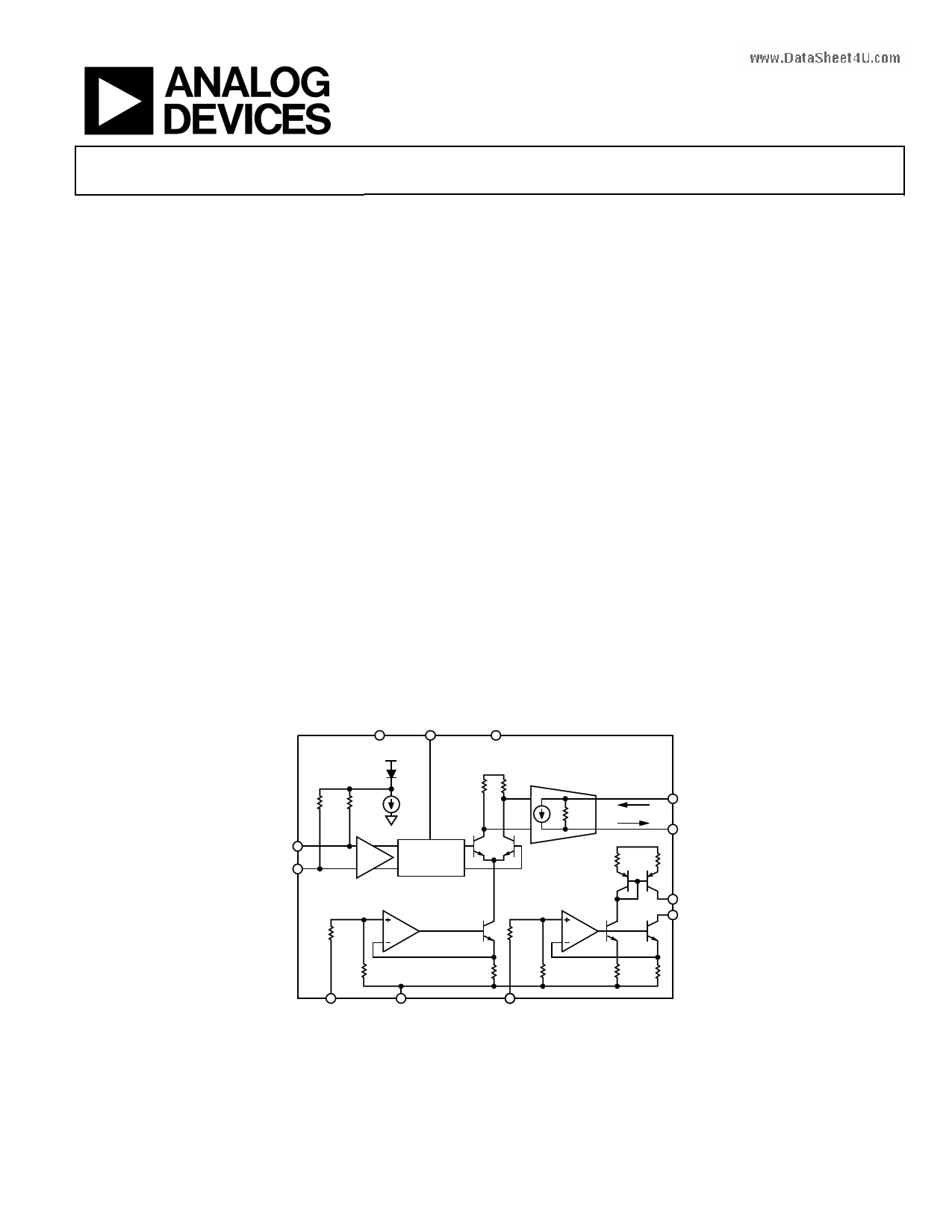
FUNCTIONAL BLOCK DIAGRAM
VCC
CPA
ALS
VCC
VCC ADN2531
50Ω 50Ω
GND
CROSSPOINT
ADJUST
100Ω
IMOD
VCC
IMODP
IMODN
400Ω
800Ω
IBMON
IBIAS
200Ω
200Ω 200Ω
10Ω
MSET
GND
BSET
Figure 1.
Rev. 0
Information furnished by Analog Devices is believed to be accurate and reliable. However, no
responsibility is assumed by Analog Devices for its use, nor for any infringements of patents or other
rights of third parties that may result from its use. Specifications subject to change without notice. No
license is granted by implication or otherwise under any patent or patent rights of Analog Devices.
Trademarksandregisteredtrademarksarethepropertyoftheirrespectiveowners.
One Technology Way, P.O. Box 9106, Norwood, MA 02062-9106, U.S.A.
Tel: 781.329.4700
www.analog.com
Fax: 781.461.3113
©2009 Analog Devices, Inc. All rights reserved.
1 page 
ABSOLUTE MAXIMUM RATINGS
Table 3.
Parameter
Supply Voltage: VCC to GND
IMODP, IMODN to GND
DATAP, DATAN to GND
All Other Pins
ESD on IMODP/IMODN1
ESD on All Other Pins1
Junction Temperature
Storage Temperature Range
1 HBM = human body model.
Rating
−0.3 V to +4.2 V
VCC − 1.5 V to 4.5 V
VCC − 1.8 V to VCC − 0.4 V
−0.3 V to VCC + 0.3 V
200 V HBM
1.5 kV HBM
150°C
−65°C to +125°C
ADN2531
Stresses above those listed under Absolute Maximum Ratings
may cause permanent damage to the device. This is a stress
rating only; functional operation of the device at these or any
other conditions above those indicated in the operational
section of this specification is not implied. Exposure to absolute
maximum rating conditions for extended periods may affect
device reliability.
ESD CAUTION
www.DataSheet4U.com
Rev. 0 | Page 5 of 20
5 Page 
THEORY OF OPERATION
As shown in Figure 1, the ADN2531 consists of an input stage and
two voltage-controlled current sources for bias and modulation.
The bias current is available at the IBIAS pin. It is controlled by the
voltage at the BSET pin and can be monitored at the IBMON pin.
The differential modulation current is available at the IMODP
and IMODN pins. It is controlled by the voltage at the MSET pin.
The output stage implements the active back-termination
circuitry for proper transmission line matching and power
consumption reduction. The ADN2531 can drive a load with
differential resistance ranging from 5 Ω to 140 Ω. The excellent
back-termination in the ADN2531 absorbs signal reflections
from the TOSA end of the output transmission lines, enabling
excellent optical eye quality to be achieved even when the
TOSA end of the output transmission lines is significantly
misterminated.
INPUT STAGE
The input stage of the ADN2531 converts the data signal applied
to the DATAP and DATAN pins to a level that ensures proper
operation of the high speed switch. The equivalent circuit of the
input stage is shown in Figure 23.
VCC
DATAP
50Ω VCC
DATAN
50Ω
www.DataSheet4U.com
Figure 23. Equivalent Circuit of the Input Stage
The DATAP and DATAN pins are terminated internally with a
100 Ω differential termination resistor. This minimizes signal
reflections at the input that could otherwise lead to degradation
in the output eye diagram. It is not recommended to drive the
ADN2531 with single-ended data signal sources.
The ADN2531 input stage must be ac-coupled to the signal source
to eliminate the need for matching between the common-mode
voltages of the data signal source and the input stage of the driver
(see Figure 24). The ac coupling capacitors should have an
impedance less than 50 Ω over the required frequency range.
Generally, this is achieved using 10 nF to 100 nF capacitors, for
more than 1 Gbps operation.
ADN2531
50Ω 50Ω
ADN2531
C
DATAP
DATAN
C
DATA SIGNAL SOURCE
Figure 24. AC Coupling the Data Source to the ADN2531 Data Inputs
BIAS CURRENT
The bias current is generated internally using a voltage-to-current
converter consisting of an internal operational amplifier and a
transistor, as shown in Figure 25.
ADN2531
VCC
BSET
800Ω
IBMON
IBMON
IBIAS
IBIAS
200Ω
200Ω
2Ω
GND
Figure 25. Voltage-to-Current Converter Used to Generate IBIAS
The BSET to IBIAS voltage-to-current conversion factor is set
at 100 mA/V by the internal resistors, and the bias current is
monitored at the IBMON pin using a current mirror with a gain
equal to 1/100. By connecting a 750 Ω resistor between IBMON
and GND, the bias current can be monitored as a voltage across
the resistor. A low temperature coefficient precision resistor must
be used for the IBMON resistor (RIBMON). Any error in the value
of RIBMON due to tolerances or drift in its value over temperature
contributes to the overall error budget for the IBIAS monitor voltage.
If the IBMON voltage is being connected to an ADC for analog-
to-digital conversion, RIBMON should be placed close to the ADC to
minimize errors due to voltage drops on the ground plane. See the
Design Example section for example calculations of the accuracy of
the IBIAS monitor as a percentage of the nominal IBIAS value.
Rev. 0 | Page 11 of 20
11 Page | ||
| Páginas | Total 20 Páginas | |
| PDF Descargar | [ Datasheet ADN2531.PDF ] | |
Hoja de datos destacado
| Número de pieza | Descripción | Fabricantes |
| ADN2530 | 11.3 Gbps Active Back-Termination | Analog Devices |
| ADN2531 | Differential Laser Diode Driver | Analog Devices |
| Número de pieza | Descripción | Fabricantes |
| SLA6805M | High Voltage 3 phase Motor Driver IC. |
Sanken |
| SDC1742 | 12- and 14-Bit Hybrid Synchro / Resolver-to-Digital Converters. |
Analog Devices |
|
DataSheet.es es una pagina web que funciona como un repositorio de manuales o hoja de datos de muchos de los productos más populares, |
| DataSheet.es | 2020 | Privacy Policy | Contacto | Buscar |