|
|
|
PDF ADN4604 Data sheet ( Hoja de datos )
| Número de pieza | ADN4604 | |
| Descripción | Digital Crosspoint Switch | |
| Fabricantes | Analog Devices | |
| Logotipo | ||
Hay una vista previa y un enlace de descarga de ADN4604 (archivo pdf) en la parte inferior de esta página. Total 30 Páginas | ||
|
No Preview Available !
4.25 Gbps,
16 × 16, Digital Crosspoint Switch
ADN4604
FEATURES
DC to 4.25 Gbps per port NRZ data rate
Programmable receive equalization
12 dB boost at 2 GHz
Compensates 40 inches of FR4 at 4.25 Gbps
Programmable transmit preemphasis/deemphasis
Up to 12 dB boost at 4.25 Gbps
Compensates 40 inches of FR4 at 4.25 Gbps
Low power: 130 mW per channel at 3.3 V (outputs enabled)
16 × 16, fully differential, nonblocking array
Double rank connection programming with dual
connection maps
Low jitter, typically 20 ps
Flexible I/O supply range
DC- or ac-coupled differential CML inputs
Programmable CML output levels
Per-lane input P/N pair inversion for routing ease
50 Ω on-chip I/O termination
Supports 8b/10b, scrambled or uncoded NRZ data
Serial (I2C slave or SPI) control interface
100-lead TQFP, Pb-free package
APPLICATIONS
Fiber optic network switching
High speed serial backplane routing to OC-48 with FEC
XAUI: 10GBASE-KX4
Gigabit Ethernet over backplane: 1000BASE-KX
1×, 2×, and 4× Fibre Channel
www.DaIntafiSnhieBeatn4dU®.com
Digital video (HDMI, DVI, DisplayPort, 3G-/HD-/SD-SDI)
Data storage networks
GENERAL DESCRIPTION
The ADN4604 is a 16 × 16 asynchronous, protocol agnostic,
digital crosspoint switch, with 16 differential PECL-/CML-
compatible inputs and 16 differential CML outputs.
The ADN4604 is optimized for nonreturn-to-zero (NRZ) sig-
naling with data rates of up to 4.25 Gbps per port. Each port
offers a fixed level of input equalization and programmable
output swing and output preemphasis.
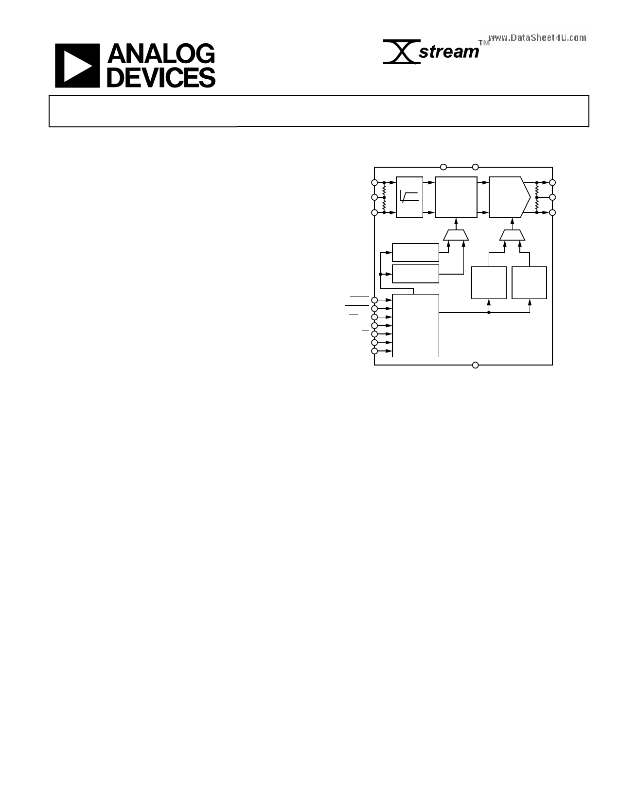
FUNCTIONAL BLOCK DIAGRAM
DVCC
VCC
IP[15:0]
VTTIE,
VTTIW
IN[15:0]
RX TX
EQ
16 × 16
SWITCH
MATRIX
PRE-
EMPHASIS
OP[15:0]
VTTON,
VTTOS
ON[15:0]
RESET
UPDATE
I2C/SPI
ADDR1/SDI
ADDR0/CS
SDA/SDO
SCL/SCK
CONNECTION
MAP 0
CONNECTION
MAP 1
SERIAL
INTERFACE
CONTROL
LOGIC
OUTPUT
LEVEL
HOOKUP
TABLE
PER-PORT
OUTPUT
LEVEL
SETTINGS
ADN4604
VEE
Figure 1.
The ADN4604 nonblocking switch core implements a 16 × 16
crossbar and supports independent channel switching through
the serial control interface. The ADN4604 has low latency and
very low channel-to-channel skew.
An I2C® or SPI interface is used to control the device and pro-
vide access to advanced features, such as additional levels of
preemphasis and output disable.
The ADN4604 is packaged in a 100-lead TQFP package and
operates from −40°C to +85°C.
Rev. 0
Information furnished by Analog Devices is believed to be accurate and reliable. However, no
responsibility is assumed by Analog Devices for its use, nor for any infringements of patents or other
rights of third parties that may result from its use. Specifications subject to change without notice. No
license is granted by implication or otherwise under any patent or patent rights of Analog Devices.
Trademarksandregisteredtrademarksarethepropertyoftheirrespectiveowners.
One Technology Way, P.O. Box 9106, Norwood, MA 02062-9106, U.S.A.
Tel: 781.329.4700
www.analog.com
Fax: 781.461.3113
©2009 Analog Devices, Inc. All rights reserved.
1 page 
SPI TIMING SPECIFICATIONS
CS
t1
t2
SCK
SDI
t3 t5 t6
A7 A6 A5 A4 A3 A2 A1 A0 D7 D6 D5 D4 D3 D2 D1
t4
SDO
XXXXXXXX XXXXXXX
Figure 3. SPI Write Timing Diagram
t7
D0
t8
X
CS
SCK
SDI
t9
t1 t2
t3 t5 t6
A7 A6 A5 A4 A3 A2 A1 A0
D7 D6 D5 D4 D3 D2 D1
t4
SDO
XXX XX XXX
D7 D6 D5 D4 D3 D2 D1
Figure 4. SPI Read Timing Diagram
t7
D0
t8
D0
ADN4604
Table 3. SPI Timing Specifications
Parameter
SCK Clock Frequency
CS to SCK Setup Time
SCK High Pulse Width
SCK Low Pulse Width
www.DaDtatSahAecect4eUss.cToime After SCK Falling Edge
Data Setup Time Prior to SCK Rising Edge
Data Hold Time After SCK Rising Edge
CS to SCK Hold Time
CS to SDO High Impedance
CS High Pulse Width
Symbol
fSCK
t1
t2
t3
t4
t5
t6
t7
t8
t9
Min Max
0 10
10
40
40
35
20
10
10
40
10
Unit
MHz
ns
ns
ns
ns
ns
ns
ns
ns
ns
Rev. 0 | Page 5 of 40
5 Page 
ADN4604
DATA OUT
PATTERN
GENERATOR
50Ω CABLES
22
TP1
50Ω CABLES
FR4 TEST BACKPLANE 2
2
DIFFERENTIAL
STRIPLINE TRACES
8mils WIDE, 8mils SPACE,
8mils DIELECTRIC HEIGHT
LENGTHS = 10 INCHES, 20 INCHES,
30 INCHES, 40 INCHES
TP2
INPUT OUTPUT
PIN PIN
ADN4604
AC-COUPLED
EVALUATION
BOARD
50Ω CABLES
22
TP3
50Ω
HIGH
SPEED
SAMPLING
OSCILLOSCOPE
0.167IU/DIV
REFERENCE EYE DIAGRAM AT TP1
Figure 11. Equalization Test Circuit
0.167IU/DIV
Figure 12. 4.25 Gbps Input Eye, 20 Inch FR4 Input Channel
(TP2 from Figure 11)
0.167IU/DIV
Figure 14. 4.25 Gbps Output Eye, 20-Inch FR4 Input Channel, EQ = 12 dB
(TP3 from Figure 11)
www.DataSheet4U.com
0.167IU/DIV
Figure 13. 4.25 Gbps Input Eye, 40-Inch FR4 Input Channel
(TP2 from Figure 11)
0.167IU/DIV
Figure 15. 4.25 Gbps Output Eye, 40-Inch FR4 Input Channel, EQ = 12 dB
(TP3 from Figure 11)
Rev. 0 | Page 11 of 40
11 Page | ||
| Páginas | Total 30 Páginas | |
| PDF Descargar | [ Datasheet ADN4604.PDF ] | |
Hoja de datos destacado
| Número de pieza | Descripción | Fabricantes |
| ADN4600 | Asynchronous Crosspoint Switch | Analog Devices |
| ADN4604 | Digital Crosspoint Switch | Analog Devices |
| ADN4605 | 4.25 Gbps 40 X 40 Digital Crosspoint Switch | Analog Devices |
| Número de pieza | Descripción | Fabricantes |
| SLA6805M | High Voltage 3 phase Motor Driver IC. |
Sanken |
| SDC1742 | 12- and 14-Bit Hybrid Synchro / Resolver-to-Digital Converters. |
Analog Devices |
|
DataSheet.es es una pagina web que funciona como un repositorio de manuales o hoja de datos de muchos de los productos más populares, |
| DataSheet.es | 2020 | Privacy Policy | Contacto | Buscar |