|
|
|
PDF DS42MB200 Data sheet ( Hoja de datos )
| Número de pieza | DS42MB200 | |
| Descripción | Dual 4.25 Gbps 2:1/1:2 CML Mux/Buffer | |
| Fabricantes | National Semiconductor | |
| Logotipo | ||
Hay una vista previa y un enlace de descarga de DS42MB200 (archivo pdf) en la parte inferior de esta página. Total 16 Páginas | ||
|
No Preview Available !
December 7, 2007
DS42MB200
Dual 4.25 Gbps 2:1/1:2 CML Mux/Buffer with Transmit Pre-
Emphasis and Receive Equalization
General Description
The DS42MB200 is a dual signal conditioning 2:1 multiplexer
and 1:2 fan-out buffer designed for use in backplane redun-
dancy applications. Signal conditioning features include input
equalization and programmable output pre-emphasis that en-
able data communication in FR4 backplanes up to 4.25 Gbps.
Each input stage has a fixed equalizer to reduce ISI distortion
from board traces.
All output drivers have 4 selectable steps of pre-emphasis to
compensate for transmission losses from long FR4 back-
planes and reduce deterministic jitter. The pre-emphasis lev-
els can be independently controlled for the line-side and
switch-side drivers. The internal loopback paths from switch-
side input to switch-side output enable at-speed system test-
ing. All receiver inputs and driver outputs are internally
terminated with 100Ω differential terminating resistors.
Features
■ 1– 4.25 Gbps fully differential data paths
■ Fixed input equalization
■ Programmable output pre-emphasis
■ Independent switch and line side pre-emphasis controls
■ Programmable switch-side loopback mode
■ On-chip terminations
■ +3.3V supply
■ ESD rating HBM 6 kV
■ Lead-less LLP-48 package (7mmx7mmx0.8mm, 0.5mm
pitch)
■ –40°C to +85°C operating temperature range
Applications
■ Backplane driver or cable driver
■ Redundancy and signal conditioning applications
■ XAUI
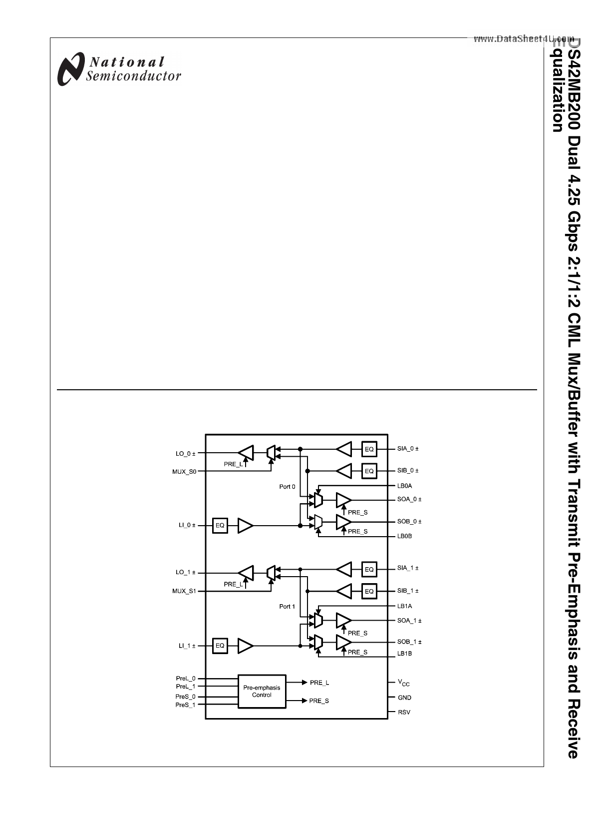
Functional Block Diagram
www.DataSheet4U.com
© 2007 National Semiconductor Corporation 201786
20178633
www.national.com
1 page 
Pin Name Pin Number I/O
Description
POWER
VCC 2, 8, 14, 20, P VCC = 3.3V ± 5%.
29, 35, 38,
Each VCC pin should be connected to the VCC plane through a low inductance path, typically with a
44 via located as close as possible to the landing pad of the VCC pin.
It is recommended to have a 0.01 μF or 0.1 μF, X7R, size-0402 bypass capacitor from each VCC
pin to ground plane.
GND
5, 11, 17, 32, P Ground reference. Each ground pin should be connected to the ground plane through a low
41 inductance path, typically with a via located as close as possible to the landing pad of the GND pin.
GND
DAP
P Die Attach Pad (DAP) is the metal contact at the bottom side, located at the center of the LLP-48
package. It should be connected to the GND plane with at least 4 via to lower the ground impedance
and improve the thermal performance of the package.
Note: I = Input, O = Output, P = Power
Functional Description
The DS42MB200 is a signal conditioning 2:1 multiplexer and
a 1:2 buffer designed to support port redundancy up to 4.25
Gbps. Each input stage has a fixed equalizer that provides
equalization to compensate about 5 dB of transmission loss
from a short backplane trace (about 10 inches backplane).
The output driver has pre-emphasis (driver-side equalization)
to compensate the transmission loss of the backplane that it
is driving. The driver conditions the output signal such that the
lower frequency and higher frequency pulses reach approxi-
mately the same amplitude at the end of the backplane, and
minimize the deterministic jitter caused by the amplitude dis-
parity. The DS42MB200 provides 4 steps of user-selectable
pre-emphasis ranging from 0, -3, -6 and –9 dB to handle dif-
ferent lengths of backplane. Figure 1 shows a driver pre-
emphasis waveform. The pre-emphasis duration is 200ps
nominal, corresponds to 0.75 bit-width at 4 Gbps. The pre-
emphasis levels of switch-side and line-side can be individu-
ally programmed.
The high speed inputs are self-biased to about 1.5V and are
designed for AC coupling. The inputs are compatible to most
AC coupling differential signals such as LVDS, LVPECL and
CML.
TABLE 1. LOGIC TABLE FOR MULTIPLEX CONTROLS
MUX_S0
0
1 (default)
MUX_S1
0
1 (default)
Mux Function
MUX_0 select switch_B input, SIB_0±.
MUX_0 select switch_A input, SIA_0±.
Mux Function
MUX_1 select switch_B input, SIB_1±.
MUX_1 select switch_A input, SIA_0±.
www.DataSheet4U.com
LB0A
0
1 (default)
LB0B
0
1 (default)
LB1A
0
1 (default)
LB1B
0
1 (default)
TABLE 2. LOGIC TABLE FOR LOOPBACK Controls
Loopback Function
Enable loopback from SIA_0± to SOA_0±.
Normal mode. Loopback disabled.
Loopback Function
Enable loopback from SIB_0± to SOB_0±.
Normal mode. Loopback disabled.
Loopback Function
Enable loopback from SIA_1± to SOA_1±.
Normal mode. Loopback disabled.
Loopback Function
Enable loopback from SIB_1± to SOB_1±.
Normal mode. Loopback disabled.
5 www.national.com
5 Page 
FIGURE 6. Data input and output eye patterns with driver set to 0 dB pre-emphasis
20178642
www.DataSheet4U.com
11 www.national.com
11 Page | ||
| Páginas | Total 16 Páginas | |
| PDF Descargar | [ Datasheet DS42MB200.PDF ] | |
Hoja de datos destacado
| Número de pieza | Descripción | Fabricantes |
| DS42MB200 | DS42MB200 Dual 4.25Gbps 2:1/1:2 CML Mux/Buffer w/Transmit Pre-Emph Rcve Equal (Rev. G) | Texas Instruments |
| DS42MB200 | Dual 4.25 Gbps 2:1/1:2 CML Mux/Buffer | National Semiconductor |
| Número de pieza | Descripción | Fabricantes |
| SLA6805M | High Voltage 3 phase Motor Driver IC. |
Sanken |
| SDC1742 | 12- and 14-Bit Hybrid Synchro / Resolver-to-Digital Converters. |
Analog Devices |
|
DataSheet.es es una pagina web que funciona como un repositorio de manuales o hoja de datos de muchos de los productos más populares, |
| DataSheet.es | 2020 | Privacy Policy | Contacto | Buscar |