|
|
|
PDF FDMF6704V Data sheet ( Hoja de datos )
| Número de pieza | FDMF6704V | |
| Descripción | High Frequency DrMOS Module | |
| Fabricantes | Fairchild Semiconductor | |
| Logotipo | ||
Hay una vista previa y un enlace de descarga de FDMF6704V (archivo pdf) en la parte inferior de esta página. Total 13 Páginas | ||
|
No Preview Available !
August 2009
FDMF6704V - XSTM DrMOS
The Xtra Small, High Performance, High Frequency DrMOS Module with LDO tm
Benefits
General Description
Single 12 V power supply operation.
Ultra compact size - 6 mm x 6 mm MLP, 44 % space
saving compared to conventional MLP 8 mm x 8 mm
DrMOS packages.
Ultra compact thermally enhanced 6 mm x 6 mm MLP
package 84 % smaller than conventional discrete solutions.
Fully optimized system efficiency.
Clean voltage waveforms with reduced ringing.
High frequency operation.
Compatible with a wide variety of PWM controllers in the
market.
Single input voltage operation.
Features
Internal 12 V to 5 V regulator.
Synchronous driver plus FET multichip module.
High current handling of 35 A.
Over 93 % peak efficiency.
Tri-State PWM input.
Fairchild's PowerTrench® 5 technology MOSFETs for clean
voltage waveforms and reduced ringing.
Optimized for high switching frequencies of up to 1 MHz.
Skip mode SMOD [low side gate turn off] input.
Fairchild SyncFETTM [integrated Schottky diode] technology
in the low side MOSFET.
Integrated bootstrap Schottky diode.
Adaptive gate drive timing for shoot-through protection.
Driver output disable function [DISB# pin].
Undervoltage lockout (UVLO).
Fairchild Green Packaging and RoHS
compliant. Low profile SMD package.
www.DataSheet4U.com
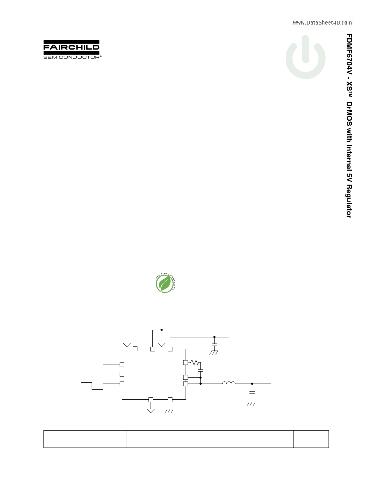
Power Train Application Circuit
CVCIN
CVDRV
The XSTM DrMOS family is Fairchild’s next-generation fully-
optimized, ultra-compact, integrated MOSFET plus driver power
stage solutions for high current, high frequency synchronous
buck DC-DC applications. The FDMF6704V XSTM DrMOS
integrates a driver IC, two power MOSFETs and a bootstrap
Schottky diode along with an integrated 5 V gate drive LDO
regulator into a thermally enhanced, ultra compact 6 mm x 6
mm MLP package. With an integrated approach, the complete
switching power stage is optimized with regards to driver and
MOSFET dynamic performance, system inductance and
RDS(ON). This greatly reduces the package parasitics and layout
challenges associated with conventional discrete solutions.
XSTM DrMOS uses Fairchild's high performance
PowerTrenchTM 5 MOSFET technology, which dramatically
reduces ringing in synchronous buck converter applications.
PowerTrenchTM 5 can eliminate the need for a snubber circuit in
buck converter applications. The driver IC incorporates
advanced features such as SMOD for improved light load
efficiency and a Tri-State PWM input for compatibility with a
wide range of PWM controllers. A 5 V gate drive and an
improved PCB interface, optimized for a maximum low side FET
exposed pad area, ensure higher performance. This product is
compatible with the new Intel 6 mm x 6 mm DrMOS
specification.
Applications
Compact blade servers V-core, non V-core and VTT DC-DC
converters.
Desktop computers V-core, non V-core and VTT DC-DC
converters.
Workstations V-core, non V-core and VTT DC-DC
converters.
Gaming Motherboards V-core, non V-core and VTT DC-DC
converters.
Gaming consoles.
High-current DC-DC Point of Load (POL) converters.
Networking and telecom microprocessor voltage regulators.
VDRV
VIN
CVIN
DISB#
PWM Input
OFF
ON
VCIN VDRV VIN
DISB#
BOOT
PWM
SMOD#
PHASE
VSWH
CGND PGND
RBOOT
CBOOT
LOUT
OUTPUT
COUT
Ordering Information
Order Number
FDMF6704V
Marking
FDMF6704V_1
Figure 1. Power Train Application Circuit
Temperature Range
-55 °C to 150 °C
Device Package
40 Pin, 3 DAP, MLP 6x6 mm
Packing Method
Tape and Reel
Quantity
3000
©2008 Fairchild Semiconductor Corporation
FDMF6704V Rev.C
1
www.fairchildsemi.com
1 page 
Description of Operation
Circuit Description
The FDMF6704V is a driver plus FET module incorporating an
internal 12 V to 5 V regulator that is optimized for synchronous
buck converter topology. A single PWM input signal is all that is
required to properly drive the high-side and the low-side
MOSFETs at speeds up to 1 MHz.
PWM
When the PWM input goes high, the high side MOSFET turns
on. When it goes low, the low side MOSFET turns on. When it is
open, both the low side and high side MOFET will turn off. The
individual PWM signals from the controller will be used to
dynamically enable or disable individual phases.
DISB#
The DISB# input is combined with the PWM signal to control the
driver output. In a typical multiphase design, DISB# will be a
common signal used to turn on all phases.
Gate Low
The low-side driver (GL) is designed to drive a ground
referenced low RDS(ON) N-channel MOSFET. The bias for GL is
internally connected between VCIN and CGND. When the
driver is enabled, the driver's output is 180° out of phase with
the PWM input. When the driver is disabled (DISB# = 0 V), GL
is held low turning the low side FET off.
Gate High
The high-side driver (GH) is designed to drive a floating
N-channel MOSFET. The bias voltage for the high-side driver is
developed by a bootstrap supply circuit, consisting of the
internal BOOT diode and an external bootstrap capacitor
(CBOOT). During start-up, VSWH is held at PGND, allowing
CBOOT to charge to VCIN through the internal diode. When the
PWM input goes high, GH will begin to charge the high-side
MOSFET's gate (Q1). During this transition, charge is removed
www.DataShfrriesoeemst4CUtoB.cOVoOmITN,anfodrcdienlgivethreed
to Q1's gate.
BOOT pin to
As Q1 turns on, VSWH
VIN +VC(BOOT), which
provides sufficient VGS enhancement for Q1. To complete the
switching cycle, Q1 is turned off by pulling GH to VSWH. CBOOT
is then recharged to VCIN when VSWH falls to PGND. GH
output is in phase with the PWM input. When the driver is
disabled, the high-side FET is turned off.
VDRV and VCIN
The FDMF6704V incorporates an internal 12 V to 5 V regulator
to allow it to be used in single 12 V supply applications.
The regulator’s 5V output (VCIN) is connected to pin 2 and used
internally to supply power to the gate drives and to the internal
logic. A 4.7 F X7R ceramic capacitor must be connected
between VCIN and ground. This capacitor is part of the
regulator’s loop compensation so a high X7R type is required.
The regulator’s input VDRV is connected to pin 3.
SMOD#
The SMOD (Skip Mode) function allows for higher converter
efficiency under light load conditions. During SMOD, the LS
FET is disabled and it prevents discharging of output caps.
When the SMOD# pin is pulled high, the sync buck converter
will work in synchronous mode. When the SMOD# pin is pulled
low, the LS FET is turned off. The SMOD function does not have
internal current sensing. This SMOD# pin is connected to a
PWM controller which enables or disables the SMOD
automatically when the controller detects light load condition.
This pin is Active Low.
Adaptive Gate Drive Circuit
The driver IC embodies an advanced design that ensures
minimum MOSFET dead-time while eliminating potential
shoot-through (cross-conduction) currents. It senses the state of
the MOSFETs and adjusts the gate drive, adaptively, to ensure
they do not conduct simultaneously. Refer to Figure 4 for the
relevant timing waveforms.
To prevent overlap during the low-to-high switching transition
(Q2 OFF to Q1 ON), the adaptive circuitry monitors the voltage
at the GL pin. When the PWM signal goes HIGH, Q2 will begin
to turn OFF after some propagation delay (tPDLL). Once the GL
pin is discharged below 1 V, Q1 begins to turn ON after adaptive
delay tDTHH.
To preclude overlap during the high-to-low transition (Q1 OFF to
Q2 ON), the adaptive circuitry monitors the voltage at the
VSWH pin. When the PWM signal goes LOW, Q1 will begin to
turn OFF after some propagation delay (tPDHL). Once the
VSWH pin falls below 1 V, Q2 begins to turn ON after adaptive
delay tDTLH.
Additionally, VGS of Q1 is monitored. When VGS(Q1) is
discharged low, a secondary adaptive delay is initiated, which
results in Q2 being driven ON after 250 ns, regardless of VSWH
state. This function is implemented to ensure CBOOT is
recharged each switching cycle, particularly for cases where the
power converter is sinking current and VSWH voltage does not
fall below the 1 V adaptive threshold. The 250 ns secondary
delay is longer than tDTLH.
5 www.fairchildsemi.com
FDMF6704V Rev. C
5 Page 
TOP VIEW
Figure 21. Typical PCB Layout Example
BOTTOM VIEW
www.DataSheet4U.com
11 www.fairchildsemi.com
FDMF6704V Rev. C
11 Page | ||
| Páginas | Total 13 Páginas | |
| PDF Descargar | [ Datasheet FDMF6704V.PDF ] | |
Hoja de datos destacado
| Número de pieza | Descripción | Fabricantes |
| FDMF6704 | High Frequency DrMOS Module | Fairchild Semiconductor |
| FDMF6704A | High Frequency DrMOS Module | Fairchild Semiconductor |
| FDMF6704V | High Frequency DrMOS Module | Fairchild Semiconductor |
| Número de pieza | Descripción | Fabricantes |
| SLA6805M | High Voltage 3 phase Motor Driver IC. |
Sanken |
| SDC1742 | 12- and 14-Bit Hybrid Synchro / Resolver-to-Digital Converters. |
Analog Devices |
|
DataSheet.es es una pagina web que funciona como un repositorio de manuales o hoja de datos de muchos de los productos más populares, |
| DataSheet.es | 2020 | Privacy Policy | Contacto | Buscar |