|
|
|
PDF PE3342 Data sheet ( Hoja de datos )
| Número de pieza | PE3342 | |
| Descripción | Integer-N PLL | |
| Fabricantes | Peregrine Semiconductor | |
| Logotipo | ||
Hay una vista previa y un enlace de descarga de PE3342 (archivo pdf) en la parte inferior de esta página. Total 17 Páginas | ||
|
No Preview Available !
Product Description
Peregrine’s PE3342 is a high performance integer-N PLL with
embedded EEPROM capable of frequency synthesis up to
2700 MHz with a speed-grade option to 3000 MHz. The
EEPROM allows designers to permanently store control bits,
allowing easy configuration of self-starting synthesizers. The
superior phase noise performance of the PE3342 is ideal for
applications such as wireless base stations, fixed wireless, and
RF instrumentation systems.
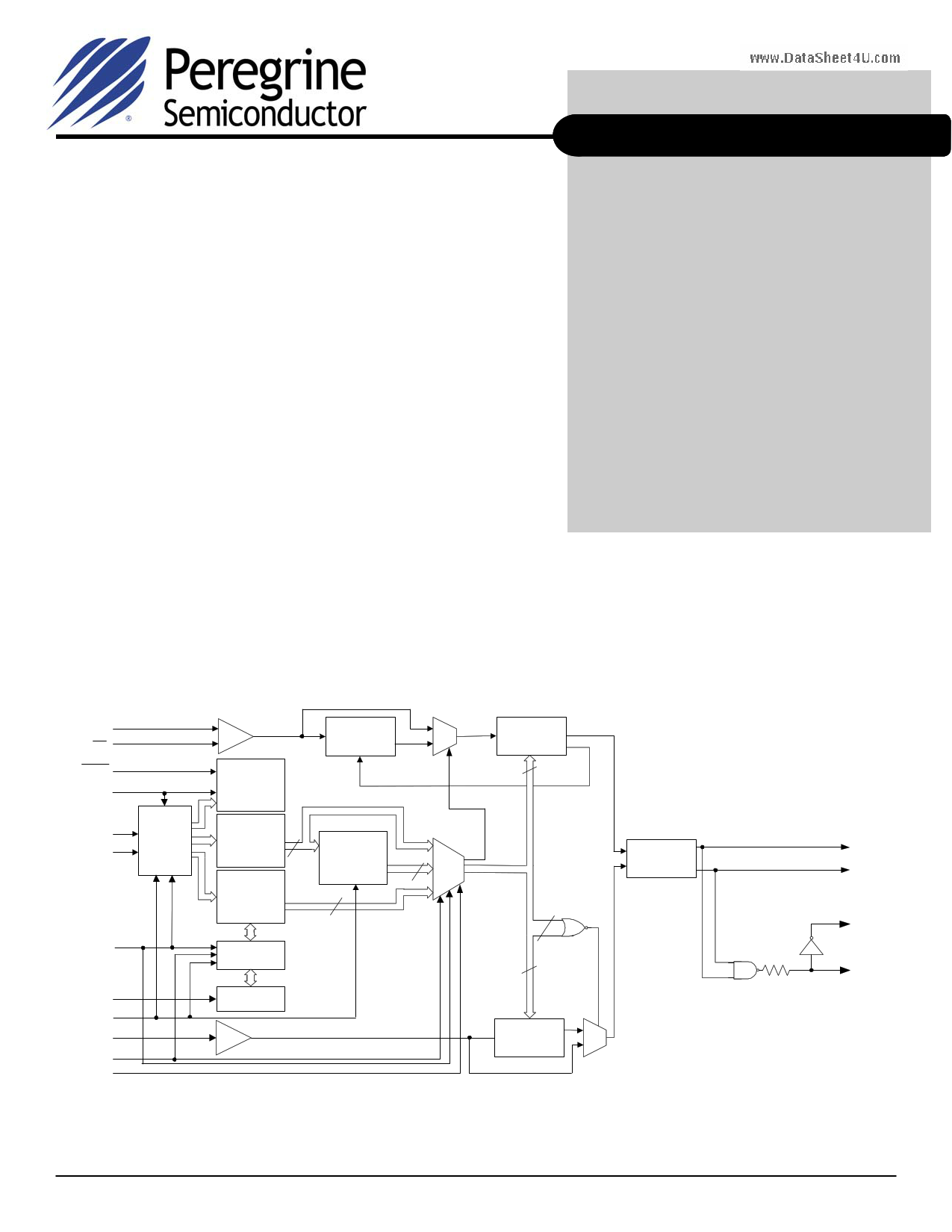
The PE3342 features a ÷10/11 dual modulus prescaler,
counters, and a phase comparator as shown in Figure 1.
Counter values are programmable through a three-wire serial
interface.
The PE3342 UltraCMOS™ Phase Locked-Loop is
manufactured in Peregrine’s patented Ultra Thin Silicon
(UTSi®) CMOS process, offering excellent RF performance
with the economy and integration of conventional CMOS.
Product Specification
PE3342
2.7 GHz Integer-N PLL
with Field-Programmable EEPROM
Features
• Field-programmable EEPROM for self-
starting applications
• Standard 2700 MHz operation,
3000 MHz speed-grade option
• ÷10/11 dual modulus prescaler
• Internal phase detector
• Serial programmable
• Low power — 20 mA at 3 V
• Ultra-low phase noise
• Available in 24-lead TSSOP or 20-lead
4x4 mm QFN package
Figure 1. Block Diagram
Fin
www.DataFSinheet4U.com
ENH
E_W R
Data
Clock
Serial
Interface
Mux
EELoad
VPP
S_W R
fr
EESel
FSel
Enhancement
Register
(8-bit)
Primary
Register
(20-bit)
EE
Register
(20-bit)
20
Transfer
Logic
Prescaler
÷10/11
Secondary
Register
(20-bit)
20
20
EEPROM
M Counter
÷2 to ÷512
13
6
6
R Counter
÷1 to ÷64
Phase
Detector
PD_U
PD_D
LD
2k
Cext
Document No. 70-0091-03 │ www.psemi.com
©2005 Peregrine Semiconductor Corp. All rights reserved.
Page 1 of 17
1 page 
PE3342
Product Specification
Table 6. AC Characteristics
VDD = 3.0 V, -40° C < TA < 85° C, unless otherwise specified
Symbol
Parameter
Conditions
Control Interface and Registers (see Figure 4)
fClk Serial data clock frequency
(Note 1)
tClkH Serial clock HIGH time
tClkL Serial clock LOW time
tDSU Data set-up time to Clock rising edge
tDHLD
Data hold time after Clock rising edge
tPW S_WR pulse width
tCWR Clock rising edge to S_WR rising edge
tCE Clock falling edge to E_WR transition
tWRC S_WR falling edge to Clock rising edge
tEC E_WR transition to Clock rising edge
EEPROM Erase/Write Programming (see Figures 5 & 6)
tEESU
tEEPW
tVPP
EELoad rising edge to VPP rising edge
VPP pulse width
VPP pulse rise and fall times
Main Divider (Including Prescaler)
(Note 2)
FIn Operating frequency
FIn Operating frequency
Speed-grade option (Note 3)
PFIn Input level range
External AC coupling
Main Divider (Prescaler Bypassed)
FIn Operating frequency
(Note 4)
PFIn Input level range
External AC coupling (Note 4)
Reference Divider
www.DataSfrheet4U.coOmperating frequency
(Note 5)
Pfr Reference input power (Note 4)
Single ended input
Phase Detector
fc Comparison frequency
(Note 6)
SSB Phase Noise (Fin = 1.3 GHz, fr = 10 MHz, fc = 1.25 MHz, LBW = 70 kHz, VDD = 3.0 V, Temp = -40° C)
100 Hz Offset
1 kHz Offset
Min
30
30
10
10
30
30
30
30
30
500
25
1
300
300
-5
50
-5
-2
Max
10
30
2700
3000
5
270
5
100
20
-75
-85
Units
MHz
ns
ns
ns
ns
ns
ns
ns
ns
ns
ns
ms
µs
MHz
MHz
dBm
MHz
dBm
MHz
dBm
MHz
dBc/Hz
dBc/Hz
Note 1:
Note 2:
fClk is verified during the functional pattern test. Serial programming sections of the functional pattern are clocked at 10 MHz to verify fClk
specification.
Rise and fall times of the VPP programming voltage pulse must be greater than 1 µs.
Note 3: The maximum frequency of operation can be extended to 3.0 GHz by ordering a special speed-grade option. Please refer to Table 14,
Ordering Information, for ordering details.
Note 4:
CMOS logic levels can be used to drive FIn input if DC coupled and used in Prescaler Bypass mode. Voltage input needs to be a minimum
of 0.5 Vp-p. For optimum phase noise performance, the reference input falling edge rate should be faster than 80 mV/ns. No minimum
frequency limit exists when operated in this mode.
Note 5: CMOS logic levels can be used to drive reference input if DC coupled. Voltage input needs to be a minimum of 0.5 Vp-p. For optimum
phase noise performance, the reference input falling edge rate should be faster than 80 mV/ns.
Note 6: Parameter is guaranteed through characterization only and is not tested.
Document No. 70-0091-03 │ www.psemi.com
©2005 Peregrine Semiconductor Corp. All rights reserved.
Page 5 of 17
5 Page 
PE3342
Product Specification
Gross EEPROM Programming Timing Grid
Figure 7 shows a gross PE3342 EEPROM
programming timing grid although each individual
step has been described thoroughly in previous
sections. It starts with EE Register load, and then
together with other parameters a Vpp_ERASE
negative pulse is applied to Vpp pin to erase the
EEPROM contents and followed by a Vpp_WRITE
pulse for EEPROM write cycle. The separation
between the Vpp_ERASE and Vpp_WRITE pulse
has to be at least 100 ms if mechanical relays are
used to avoid both being on at the same time.
After EE programming, the contents of the
EEPROM cells can be verified by setting
Enhancement Register Bit 1. A procedure shown
in Figure 8 is applied twice. The first time is to
load the EE Register from EEPROM and the
second time is to shift out the EE Register
contents through Dout pin.
Figure 7. Gross PE3342 EEPROM Programming Timing Grid
EELoa
d
EESel
S_WR
E_WR
Data
www.DataSheet4U.com
Clock
Dout
3V
0V
3V
0V
3V
0V
3V
0V
3V
0V
3V
0V
3V
0V
>=100 ms
CHANNEL
CODE
ENH code set's
Dout mux to EE
0V
Vpp_ERASE
-8.5V
12.5V
Vpp_WRITE
0V
25 ms
25 ms
EE Register
load
EE PROM
Erase
EE PROM
W rite
Rough time scale
40 ms
Note: ENH/ ( Pin 3 in TSSOP or Pin 20 in QFN) is at
low (0) for this process.
The final set
of Dout is
EEPROM
content
EE Register
load from
EEPROM
EE Register
shifted out
through Dout
Document No. 70-0091-03 │ www.psemi.com
©2005 Peregrine Semiconductor Corp. All rights reserved.
Page 11 of 17
11 Page | ||
| Páginas | Total 17 Páginas | |
| PDF Descargar | [ Datasheet PE3342.PDF ] | |
Hoja de datos destacado
| Número de pieza | Descripción | Fabricantes |
| PE3340 | Integer-N PLL | Peregrine Semiconductor |
| PE3341 | Integer-N PLL | Peregrine Semiconductor |
| PE3342 | Integer-N PLL | Peregrine Semiconductor |
| Número de pieza | Descripción | Fabricantes |
| SLA6805M | High Voltage 3 phase Motor Driver IC. |
Sanken |
| SDC1742 | 12- and 14-Bit Hybrid Synchro / Resolver-to-Digital Converters. |
Analog Devices |
|
DataSheet.es es una pagina web que funciona como un repositorio de manuales o hoja de datos de muchos de los productos más populares, |
| DataSheet.es | 2020 | Privacy Policy | Contacto | Buscar |