|
|
|
PDF L9929 Data sheet ( Hoja de datos )
| Número de pieza | L9929 | |
| Descripción | SPI CONTROLLED H-BRIDGE | |
| Fabricantes | STMicroelectronics | |
| Logotipo | ||
Hay una vista previa y un enlace de descarga de L9929 (archivo pdf) en la parte inferior de esta página. Total 23 Páginas | ||
|
No Preview Available !
L9929
1 Features
■ OPERATING SUPPLY VOLTAGE 5V TO 28V
■ TYPICAL RDSon = 150 mΩ FOR EACH
OUTPUT TRANSISTOR (AT 25°C)
■ CONTINOUS DC LOAD CURRENT 5A
(Tcase < 100 °C)
■ OUTPUT CURRENT LIMITATION AT TYP.
8.6A
■ SHORT CIRCUIT SHUT DOWN FOR OUTPUT
CURRENTS OVER TYP. 10.6A
■ LOGIC- INPUTS TTL/CMOS-COMPATIBLE
■ OPERATING-FREQUENCY UP TO 30 kHz
■ OVER TEMPERATURE PROTECTION
■ SHORT CIRCUIT PROTECTION
■ UNDERVOLTAGE DISABLE FUNCTION
■ DIAGNOSTIC BY SPI OR STATUS-FLAG
(CONFIGURABLE)
■ ENABLE AND DISABLE INPUT
■ SO20 POWER PACKAGE
2 Description
The L9929 is an SPI controlled H-Bridge, de-
signed for the control of DC and stepper motors in
safety critical applications and under extreme en-
vironmental conditions.
www.DataSheet4U.com
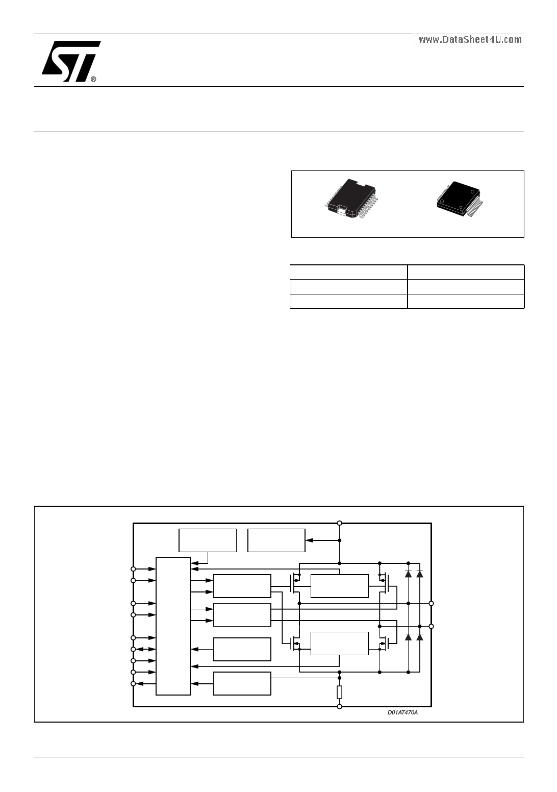
Figure 2. Block Diagram
SPI CONTROLLED H-BRIDGE
PRELIMINARY DATA
Figure 1. Package
PowerSO20
PowerSSO24
Table 1. Order Codes
Part Number
L9929
L9929XP
Package
PowerSO20
PowerSSO24
The H-Bridge is protected against over tempera-
ture and short circuits and has an under voltage
lockout for all the supply voltages "VS" (Main DC
power supply). All malfunctions cause the output
stages to go tristate.
The H-Bridge contains integrated free-wheel di-
odes. In case of free-wheeling condition, the low
side transistor is switched on in parallel of its diode
to reduce the current injected into the substrate.
Switching in parallel is only allowed, if the voltage
level of the according output-stage is below the
ground-level. In this case it must be ensured, that
the upper transistor is switched off.
VS
UNDERVOLTAGE
VS
INTERNAL 5V
SUPPLY
IN1
IN2
DI
EN
DMS
SF/SCK
SS
SI
SO
LOGIC
GATE CONTROL
1
GATE CONTROL
2
OVER
TEMPERATURE
MAXIMUM
CURRENT
LIMITATION
OVERCURRENT
HIGH-SIDE
OVERCURRENT
LOW-SIDE
OUT1
OUT2
GND
D01AT470A
May 2005
Rev. 2
1/23
This is preliminary information on a new product now in development or undergoing evaluation. Details are subject to change without notice.
1 page 
L9929
Table 6. Electrical Characteristcs (continued)
( Tj = -40 to +150°C; VS = 5 to 28V)
Symbol
Parameter
Test Condition
Min. Typ. Max. Unit
Logic inputs
VIH Logic Input Voltage High
IN1, IN2, DI, EN
2.14
V
VIL Logic Input Voltage Low
IN1, IN2, DI, EN
0.86 V
VH Logic Input Voltage Hysteresis
IN1, IN2, DI, EN
0.1 0.6 V
II Logic Input Current
IN1, IN2, DI
VI ≤ 1V
-200 -125
µA
IEN Logic Input Current EN
VIEN ≥ 1V
100 µA
tdt Detection Time EN, DI
3 4 µs
Power Outputs (OUT1, OUT2)
RS Switch on Resistance LS
ROUT-Vs, VS > 5 V
150 250 mΩ
Switch on Resistance HS
ROUT-GND, VS > 5 V
150 250 mΩ
|IOU|max Switch-off Current (*)
-40 °C < Tj < 165 °C
Tj < 175 °C
7.8 8.6 10.5(tbd) A
2.5 A
ta Switch-off time
12 17 22 µs
tb Blanking time
8 11.5 15
µs
ta/tb Tracking
1.3 1.5 1.7
|IOUK| Short circuit detection current (*)
8.9 10.6
-
A
∆|IOUK| Short Circuit Current Trecking (*)
1.3 2.0
-
A
t Reactivation time after internal Overcurrent- or overtemperature
shut down
shut down to reactivation of the
output stage
200 µs
IL Leakage Current
Output stage switched off
1 mA
VFD Free-wheel diode forward voltage IO = 3A, VS = 0V
2V
ISF Output„high“ (SF not set)
VSF = 5V
20 µA
ISF Output„low“ (SF set)
www.DataSheet4U.com
VSF = 0.5V
VSF = 0.8V
350 µA
400 µA
VSF = 1V
400 µA
Timing
f Maximum PWM Frequency
min. operating time 10µs
Device can not be controlled with
higher frequency (specify in max
ratings?)
2 30 kHz
fS Switching Frequency during
current limitation
f = 1/(ta+tb)
20 50 kHz
tdon Output ON-delay
IN1 --> OUT1 or IN2 --> OUT2
3 7.5 µs
tdoff Output OFF-delay
3 5 µs
tr Output rise time
tf Outout fall time
OUT1H--> OUT1L, OUT2H--> OUT2L,
IOUT = 3 A
OUT1L--> OUT1H, OUT2L--> OUT2H
1 5 µs
1 3 µs
tddis Disable Delay Time
DI --> OUTn, En --> OUTn
3 7 µs
tdp Power on Delay Time
VS = on --> output stage active
1 ms
terr Delay time for fault detection
1 6 µs
(*) In case of SC OUTx to gnd resp. to VS the SC switch off current is always higher than the start value of current regulation (∆|IOUK| = |IOUK|
- |IOUmax|
5/23
5 Page 
L9929
4 Diagnostic
The Diagnosis-Mode can be selected between SPI-Diagnosis and Status-Flag Diagnosis.
The choise of the Diagnosis-Mode is selected by the voltage-level on pin 12 (DMS Diagnosis Mode Selection).
DMS = GND Status-Flag
DMS = Vcc SPI-Diagnostic
For the connection of pins SI, SO, SS and SCK/SF see Fig. 13 respectively Fig. 14.
4.1 Status-Flag
The Status-Flag showes the condition „tristate“.
At the following fault-cases the output-stages switches in tristate and set the status-flag from high to low.
- Short circuit of OUT1 or OUT2 against VS or GND
- Short circuit between OUT1 and OUT2
- Overcurrent
- Overtemperature
- Undervoltage on VS
In cause of short circuit or overcurrent, the fault will be stored.
The output stage switches in tristate and the status-flag is set from high level to low-level if the specified value
is exceeded.
If the voltage level changes from high to low on DI or from low to high on EN, the output stage switches on again
and the status-flag is reset to high-level.
In cause of overtemperature the fault will be stored.
The output stage switches in tristate and the status-flag is set from high level to low-level if the specified value
is exceeded.
If the voltage level changes from high to low on DI or from low to high on EN, the output stage switches on again
and the status-flag is reset to high-level.
In cause of undervoltage on VBatt the output stage switches in tristate and the status-flag is set from high level
to low-level if the specified value is fallen. If the voltage has risen about the specified value again, the output
stage switches on again and the status-flag is reset to high-level.
The maximum current which can flow under normal operating conditions is limited to typical Imax. = 8.6A .
wWAwcwhc.eoDnradttaihnSeghemtoeat4txhUime.coutimmmec-ucrornesnttavnat ltuheeiscurreraecnht edde,ctrheeasoeustpeuxtpsotnaegnestiaallryeusnwtiiltcthheednetrxisttsawteitfcohr-oanfioxecdcutrims.e.
At the end if the fixed time the output stage switches on again and the status-flag is reset to high-level.
5 SPI-INTERFACE
5.1 General Discription
The serial SPI interface establishes a communication link between L9929 and the systems microcontroller.
L9929 always operates in slave mode whereas the controller provides the master function.
The maximum baud rate is 2 MBaud (200pF).
Applying an active slave select signal at SS L9929 is selected by the SPI master. SI is the data input (Slave In),
SO the data output (Slave Out). Via SCK (Serial Clock Input) the SPI clock is provided by the master.
In case of inactive slave select signal (High) the data output SO goes into tristate.
11/23
11 Page | ||
| Páginas | Total 23 Páginas | |
| PDF Descargar | [ Datasheet L9929.PDF ] | |
Hoja de datos destacado
| Número de pieza | Descripción | Fabricantes |
| L9925 | DMOS DUAL FULL BRIDGE DRIVER | STMicroelectronics |
| L9929 | SPI CONTROLLED H-BRIDGE | STMicroelectronics |
| Número de pieza | Descripción | Fabricantes |
| SLA6805M | High Voltage 3 phase Motor Driver IC. |
Sanken |
| SDC1742 | 12- and 14-Bit Hybrid Synchro / Resolver-to-Digital Converters. |
Analog Devices |
|
DataSheet.es es una pagina web que funciona como un repositorio de manuales o hoja de datos de muchos de los productos más populares, |
| DataSheet.es | 2020 | Privacy Policy | Contacto | Buscar |