|
|
|
PDF AD9267 Data sheet ( Hoja de datos )
| Número de pieza | AD9267 | |
| Descripción | 640 MSPS Dual Continuous Time Sigma-Delta Modulator | |
| Fabricantes | Analog Devices | |
| Logotipo | ||
Hay una vista previa y un enlace de descarga de AD9267 (archivo pdf) en la parte inferior de esta página. Total 24 Páginas | ||
|
No Preview Available !
10 MHz Bandwidth, 640 MSPS
Dual Continuous Time Sigma-Delta Modulator
AD9267
FEATURES
SNR: 83 dB (85 dBFS) to 10 MHz input
SFDR: −88 dBc to 10 MHz input
Noise figure: 15 dB
Input impedance: 1 kΩ
Power: 416 mW
10 MHz real or 20 MHz complex bandwidth
1.8 V analog supply operation
On-chip PLL clock multiplier
On-chip voltage reference
Twos complement data format
640 MSPS, 4-bit LVDS data output
Serial control interface (SPI)
APPLICATIONS
Baseband quadrature receivers: CDMA2000, W-CDMA,
multicarrier GSM/EDGE, 802.16x, and LTE
Quadrature sampling instrumentation
GENERAL DESCRIPTION
The AD9267 is a dual continuous time (CT) sigma-delta (Σ-Δ)
modulator with −88 dBc of dynamic range over 10 MHz real
or 20 MHz complex bandwidth. The combination of high
dynamic range, wide bandwidth, and characteristics unique
to the continuous time Σ-Δ modulator architecture makes the
AD9267 an ideal solution for wireless communication systems.
The AD9267 has a resistive input impedance that significantly
relaxes the requirements of the driver amplifier. In addition, a
32× oversampled fifth-order continuous time loop filter attenuates
out-of-band signals and aliases, reducing the need for external
filters at the input. The low noise figure of 15 dB relaxes the
linearity requirements of the front-end signal chain components,
and the high dynamic range reduces the need for an automatic
gain control (AGC) loop.
A differential input clock controls all internal conversion cycles.
An external clock input or the integrated integer-N PLL provides
the 640 MHz internal clock needed for the oversampled conti-
nuous time Σ-Δ modulator. The digital output data is presented
as 4-bit, LVDS at 640 MSPS in twos complement format. A data
clock output (DCO) is provided to ensure proper latch timing
with receiving logic. Additional digital signal processing may be
required on the 4-bit modulator output to remove the out-of-band
noise and to reduce the sample rate.
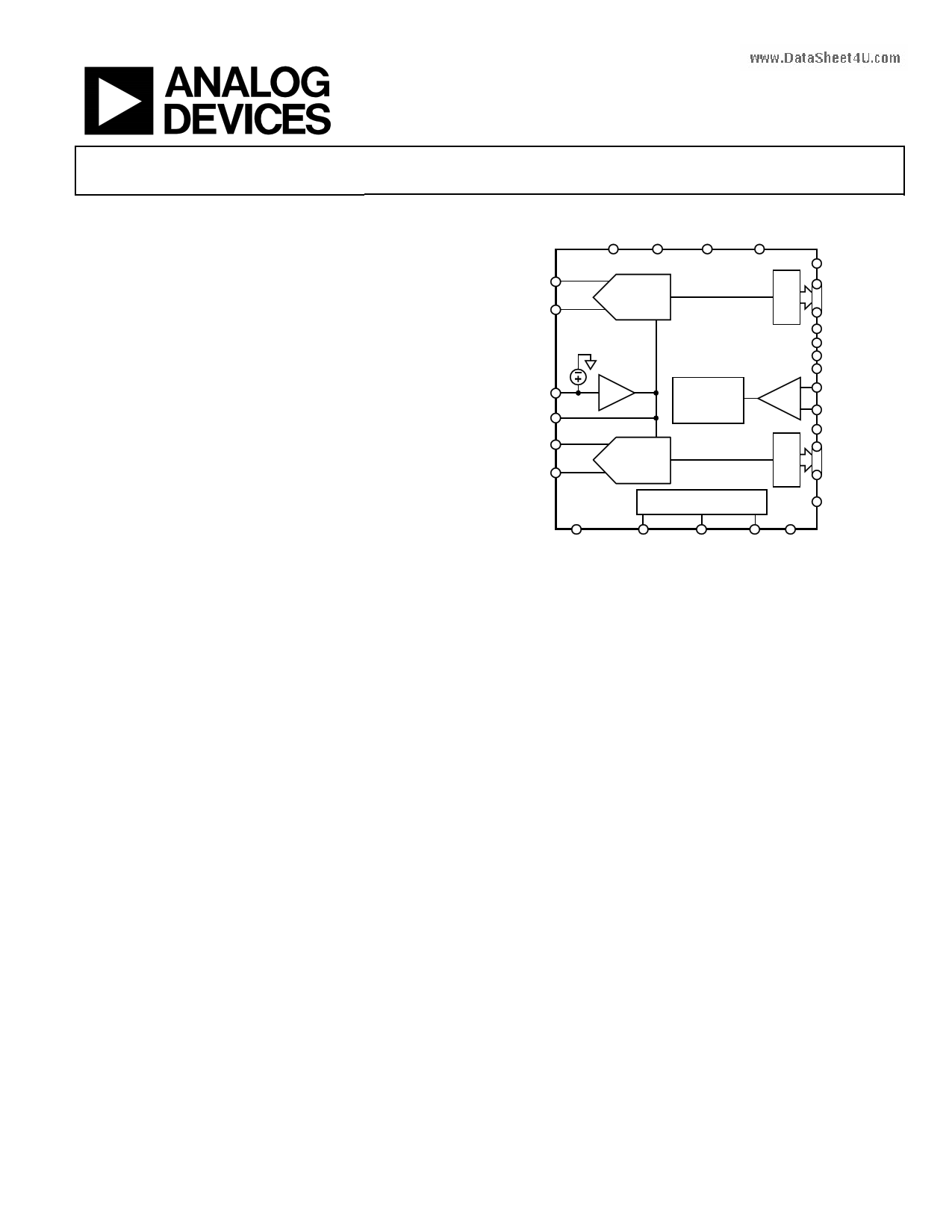
VIN+A
VIN–A
VREF
CFILT
VIN–B
VIN+B
FUNCTIONAL BLOCK DIAGRAM
AVDD PDWNB PDWNA DRVDD
Σ -Δ
MODULATOR
AD9267
PHASE-
LOCKED
LOOP
Σ -Δ
MODULATOR
SERIAL
INTERFACE
OR±A
D3±A
D0±A
PLL_LOCKED
PLLMULT4
PLLMULT3
PLLMULT2
CLK+
CLK–
DCO±
D3±B
D0±B
OR±B
AGND
SDIO/
SCLK/
PLLMULT1 PLLMULT0
Figure 1.
CSB
DGND
The AD9267 operates on a 1.8 V power supply, consuming
416 mW. The AD9267 is available in a 64-lead LFCSP and
is specified over the industrial temperature range (−40°C
to +85°C).
PRODUCT HIGHLIGHTS
1. Continuous time Σ-Δ architecture efficiently achieves high
dynamic range and wide bandwidth.
2. Passive input structure reduces or eliminates the require-
ments for a driver amplifier.
3. An oversampling ratio of 32× and high order loop filter
provide excellent alias rejection, reducing or eliminating
the need for antialiasing filters.
4. Operates from a single 1.8 V power supply.
5. A standard serial port interface (SPI) supports various
product features and functions.
6. Features a low pin count, high speed LVDS interface with
data output clock.
www.DataSheet4U.com
Rev. 0
Information furnished by Analog Devices is believed to be accurate and reliable. However, no
responsibility is assumed by Analog Devices for its use, nor for any infringements of patents or other
rights of third parties that may result from its use. Specifications subject to change without notice. No
license is granted by implication or otherwise under any patent or patent rights of Analog Devices.
Trademarksandregisteredtrademarksarethepropertyoftheirrespectiveowners.
One Technology Way, P.O. Box 9106, Norwood, MA 02062-9106, U.S.A.
Tel: 781.329.4700
www.analog.com
Fax: 781.461.3113
©2009 Analog Devices, Inc. All rights reserved.
1 page 
AD9267
DIGITAL SPECIFICATIONS
All power supplies set to 1.8 V, 640 MHz sample rate, 2 V p-p differential input, 0.5 V internal reference, PLL disabled, AIN = −2.0 dBFS,
unless otherwise noted.
Table 3.
Parameter
DIFFERENTIAL CLOCK INPUTS (CLK+, CLK−)
Logic Compliance
Differential Input Voltage
Input Common-Mode Range
High Level Input Current
Low Level Input Current
Input Resistance
Input Capacitance
LOGIC INPUTS (SCLK)
High Level Input Voltage
Low Level Input Voltage
High Level Input Current
Low Level Input Current
Input Resistance
Input Capacitance
LOGIC INPUTS (SDIO, CSB, RESET)
High Level Input Voltage
Low Level Input Voltage
High Level Input Current
Low Level Input Current
Input Resistance
Input Capacitance
DIGITAL OUTPUTS (D0±x to D3±x)
ANSI-644
Logic Compliance
Differential Output Voltage (VOD)
Output Offset Voltage (VOS)
Output Coding (Default)
Low Power, Reduced Signal Option
Logic Compliance
Differential Output Voltage (VOD)
Output Offset Voltage (VOS)
Output Coding (Default)
Temp
Min
Full 0.4
Full
Full −60
Full −60
Full
Full
Full 1.2
Full 0
Full −50
Full −10
Full
Full
Full 1.2
Full 0
Full −10
Full +40
Full
Full
Typ Max
CMOS1/LVDS/LVPECL
0.8 2
450
+60
+60
20
1
DRVDD + 0.3
0.8
−75
+10
30
2
DRVDD + 0.3
0.8
+10
+135
26
5
LVDS
Full 247
Full 1.125
Twos complement
LVDS
Full 150
Full 1.10
Twos complement
454
1.375
250
1.30
Unit
V p-p
mV
μA
μA
kΩ diff
pF
V
V
μA
μA
kΩ
pF
V
V
μA
μA
kΩ
pF
mV
V
mV
V
1 For voltage swings beyond the specified range, clamping diodes are recommended.
www.DataSheet4U.com
Rev. 0 | Page 5 of 24
5 Page 
–40
–50
–60 SFDR (dBc)
–70
–80
–90
–100
SFDR (dBFS)
–110
–120
–60
–50 –40 –30 –20
INPUT AMPLITUDE (dBFS)
–10
Figure 16. Two-Tone SFDR vs. Input Amplitude with
fIN1 = 2.1 MHz, fIN2 = 2.4 MHz
–40
–50
–60
SFDR (dBc)
–70
–80
–90
–100
–110
SFDR (dBFS)
–120
–60
–50 –40 –30 –20
INPUT AMPLITUDE (dBFS)
–10
Figure 17. Two-Tone SFDR vs. Input Amplitude with
fIN1 = 7.2 MHz, fIN2 = 8.4 MHz
AD9267
84
83 2.4MHz
82 8.4MHz
81
80
79
78
4.0 5.0 7.0 8.0 9.0 10.5 12.5 15.0 17.0
4.5 6.0 7.5 8.5 10.0 12.0 14.0 16.0 21.0
PLL DIVIDE RATIO
Figure 18. Single-Tone SNR vs. PLL Divide Ratio with
fIN1 = 2.4 MHz, fIN2 = 8.4 MHz
0.5
0
–0.5
–1.0
–1.5
–2.0
–2.5
–3.0
0
8192 16,384 24,576 32,768 40,960 49,152 57,344 65,536
OUTPUT CODE
Figure 19. INL with fIN = 2.4 MHz
www.DataSheet4U.com
Rev. 0 | Page 11 of 24
11 Page | ||
| Páginas | Total 24 Páginas | |
| PDF Descargar | [ Datasheet AD9267.PDF ] | |
Hoja de datos destacado
| Número de pieza | Descripción | Fabricantes |
| AD9260 | High Speed Oversampling CMOS ADC | Analog Devices |
| AD9261 | 30 MSPS to 160 MSPS Continuous Time Sigma-Delta ADC | Analog Devices |
| AD9262 | 30 MSPS to 160 MSPS Dual Continuous Time Sigma-Delta ADC | Analog Devices |
| AD9265 | 1.8V Analog-to-Digital Converter | Analog Devices |
| Número de pieza | Descripción | Fabricantes |
| SLA6805M | High Voltage 3 phase Motor Driver IC. |
Sanken |
| SDC1742 | 12- and 14-Bit Hybrid Synchro / Resolver-to-Digital Converters. |
Analog Devices |
|
DataSheet.es es una pagina web que funciona como un repositorio de manuales o hoja de datos de muchos de los productos más populares, |
| DataSheet.es | 2020 | Privacy Policy | Contacto | Buscar |