|
|
|
PDF LF9501 Data sheet ( Hoja de datos )
| Número de pieza | LF9501 | |
| Descripción | Programmable Line Buffer | |
| Fabricantes | LOGIC Devices Incorporated | |
| Logotipo | ||
Hay una vista previa y un enlace de descarga de LF9501 (archivo pdf) en la parte inferior de esta página. Total 7 Páginas | ||
|
No Preview Available !
DEVICES INCORPORATED
DEVICES INCORPORATED
LF9501
ProgrammabLleFLi9ne5B0u1ffer
Programmable Line Buffer
FEATURES
DESCRIPTION
u 50 MHz Maximum Operating
Frequency
u Programmable Buffer Length from
2 to 1281 Clock Cycles
u 10-bit Data Inputs and Outputs
u Data Delay and Data Recirculation
Modes
u Supports Positive or Negative Edge
System Clocks
u Expandable Data Word Width or
Buffer Length
u Replaces Harris HSP9501
u 44-pin PLCC, J-Lead
The LF9501 is a high-speed, 10-bit
programmable line buffer. Some
applications the LF9501 is useful for
include sample rate conversion, data
time compression/expansion, soft-
ware controlled data alignment, and
programmable serial data shifting. By
using the MODSEL pin, two different
modes of operation can be selected:
delay mode and data recirculation
mode. The delay mode provides a
minimum of 2 to a maximum of 1281
clock cycles of delay between the
input and output of the device. The
data recirculation mode provides a
feedback path from the data output to
the data input for use as a program-
mable circular buffer.
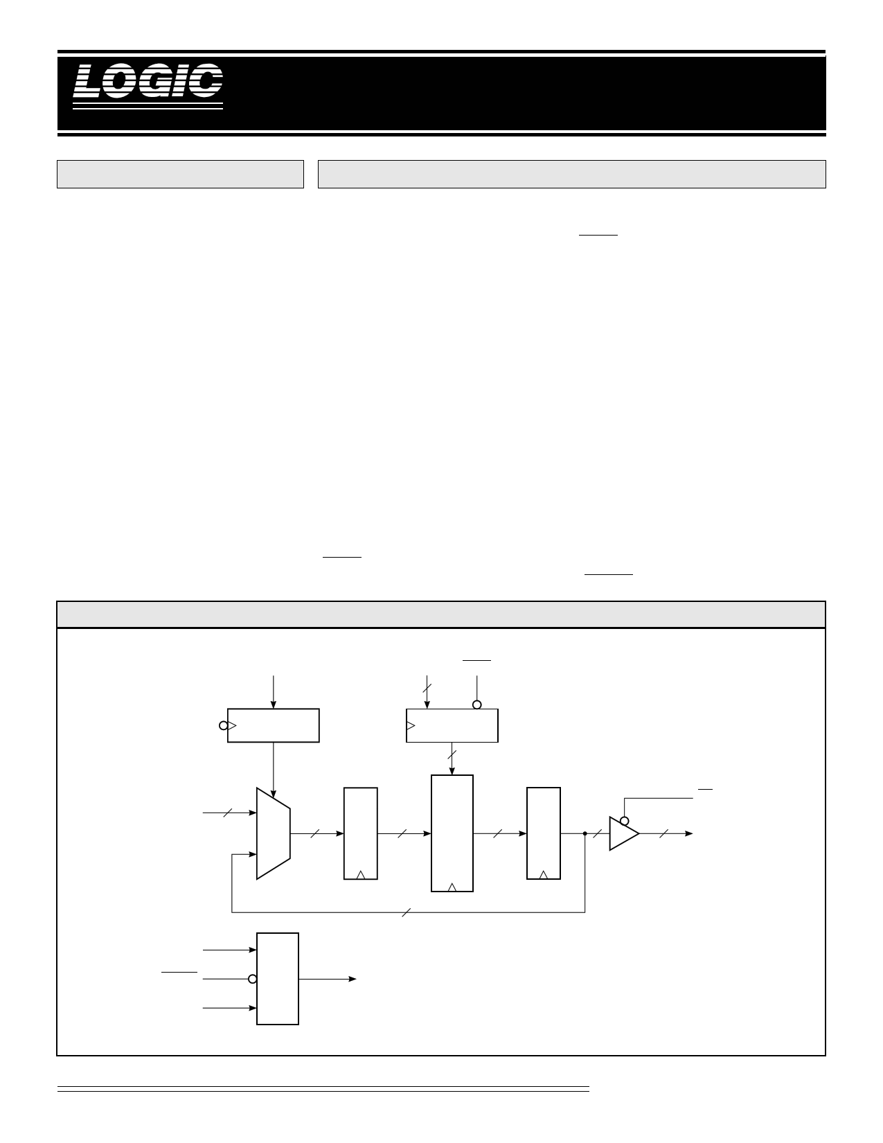
By using the length control input
(LC10-0) and the length control enable
(LCEN) the length of the delay buffer
or amount of recirculation delay can
be programmed. Providing a delay
value on the LC10-0 inputs and driving
LCEN LOW will load the delay value
into the length control register on the
next selected clock edge. Two regis-
ters, one preceeding the program-
mable delay RAM and one following,
are included in the delay path. There-
fore, the programmed delay value
should equal the desired delay minus
2. This consequently means that the
value loaded into the length control
register must range from 0 to 1279 (to
provide an overall range of 2 to 1281).
The active edge of the clock input,
either positive or negative edge, can
be selected with the clock select
(CLKSEL) input. All timing is based
on the active clock edge selected by
CLKSEL. Data can be held tempo-
rarily by using the clock enable
(CLKEN) input.
LF9501 BLOCK DIAGRAM
MODSEL
REGISTER
10
DI9-0
10
LCO10-0 LCEN
11
REGISTER
11
10 10
OE
10 10
DO9-0
CLKSEL
CLKEN
CLK
10
TO ALL REGISTERS
Video Imaging Products
1 08/16/2000–LDS.9501-H
1 page 
DEVICES INCORPORATED
LF9501
Programmable Line Buffer
SWITCHING CHARACTERISTICS
COMMERCIAL OPERATING RANGE (0°C to +70°C) Notes 9, 10 (ns)
Symbol Parameter
tCYC Cycle Time
tPW Clock Pulse Width
tDS Data Input Setup Time
tDH Data Input Hold Time
tES Clock Enable to Clock Setup Time
tEH Clock Enable to Clock Hold Time
tLS Length Control Input Setup Time
tLH Length Control Input Hold Time
tLES Length Control Enable to Clock Setup Time
tLEH Length Control Enable to Clock Hold Time
tMS Mode Select Setup Time
tMH Mode Select Hold Time
tOUT Clock to Data Out
tOH Output Hold Time (Note 8)
tENA Three-State Output Enable Delay (Note 11)
tDIS Three-State Output Disable Delay (Note 11)
111111111111111111111111111111111111111111111111111111111222222222222222222222222222222222222222222222222222222222M3333333333333333333333333333333333333333333333333333333331411111i4444444444444444444444444444444444444444444444444444444442202453232322n45555555555555555555555555555555555555555555555555555555550666666666666666666666666666666666666666666666666666666666*M777777777777777777777777777777777777777777777777777777777222888888888888888888888888888888888888888888888888888888888a255999999999999999999999999999999999999999999999999999999999x000000000000000000000000000000000000000000000000000000000111111111111111111111111111111111111111111111111111111111M2222222222222222222222222222222222222222222222222222222221311111333333333333333333333333333333333333333333333333333333333i2012420002022n44444444444444444444444444444444444444444444444444444444435555555555555555555555555555555555555555555555555555555551666666666666666666666666666666666666666666666666666666666*M777777777777777777777777777777777777777777777777777777777122a888888888888888888888888888888888888888888888888888888888604x999999999999999999999999999999999999999999999999999999999000000000000000000000000000000000000000000000000000000000LM21Fi2582402888822n92550M1111a–555x
20
Min Max
20
8
6
2
6
2
6
2
6
2
6
2
14
4
14
14
111111111111111111111111111111111111111111111111111111111M2222222222222222222222222222222222222222222222222222222221333333333333333333333333333333333333333333333333333333333i0550406555500n44444444444444444444444444444444444444444444444444444444415555555555555555555555555555555555555555555555555555555555666666666666666666666666666666666666666666666666666666666*M777777777777777777777777777777777777777777777777777777777111a888888888888888888888888888888888888888888888888888888888022x999999999999999999999999999999999999999999999999999999999000000000000000000000000000000000000000000000000000000000
CLOCK ENABLE TIMING — CLKSEL LOW
CLK*
CLKEN
tES
tPW tES
tMH
INTERNAL
CLOCK
LENGTH CONTROL TIMING — CLKSEL LOW
CLK*
LCEN
LC10-0
tLES
tLS
tLEH
tLH
tMH
111**222WD333hI444Se555Cn666OC777NL888TKI999NS000UE111EL222D333isS444PH555EI666GE777DH888,999Ga000sR111sA222uD333mE444e CLK is inverted.
5
Video Imaging Products
08/16/2000–LDS.9501-H
5 Page | ||
| Páginas | Total 7 Páginas | |
| PDF Descargar | [ Datasheet LF9501.PDF ] | |
Hoja de datos destacado
| Número de pieza | Descripción | Fabricantes |
| LF9501 | Programmable Line Buffer | LOGIC Devices Incorporated |
| LF9501JC20 | Programmable Line Buffer | LOGIC Devices Incorporated |
| LF9501JC25 | Programmable Line Buffer | LOGIC Devices Incorporated |
| LF9502 | 2K Programmable Line Buffer | LOGIC Devices Incorporated |
| Número de pieza | Descripción | Fabricantes |
| SLA6805M | High Voltage 3 phase Motor Driver IC. |
Sanken |
| SDC1742 | 12- and 14-Bit Hybrid Synchro / Resolver-to-Digital Converters. |
Analog Devices |
|
DataSheet.es es una pagina web que funciona como un repositorio de manuales o hoja de datos de muchos de los productos más populares, |
| DataSheet.es | 2020 | Privacy Policy | Contacto | Buscar |