|
|
PDF AD9573 Data sheet ( Hoja de datos )
| Número de pieza | AD9573 | |
| Descripción | PCI-Express Clock Generator IC | |
| Fabricantes | Analog Devices | |
| Logotipo |  |
|
Hay una vista previa y un enlace de descarga de AD9573 (archivo pdf) en la parte inferior de esta página. Total 12 Páginas | ||
|
No Preview Available !
www.DataSheet4U.com
FEATURES
Fully integrated VCO/PLL core
0.54 ps rms jitter from 12 kHz to 20 MHz
Input crystal frequency of 25 MHz
Preset divide ratios for 100 MHz, 33.33 MHz
LVDS/LVCMOS output format
Integrated loop filter
Space saving 4.4 mm × 5.0 mm TSSOP
0.235 W power dissipation
3.3 V operation
APPLICATIONS
Line cards, switches, and routers
CPU/PCIe applications
Low jitter, low phase noise clock generation
PCI-Express Clock Generator IC,
PLL Core, Dividers, Two Outputs
AD9573
GENERAL DESCRIPTION
The AD9573 provides a highly integrated, dual output clock
generator function including an on-chip PLL core that is
optimized for PCI-e applications. The integer-N PLL design
is based on the Analog Devices, Inc., proven portfolio of high
performance, low jitter frequency synthesizers to maximize line
card performance. Other applications with demanding phase
noise and jitter requirements also benefit from this part.
The PLL section consists of a low noise phase frequency
detector (PFD), a precision charge pump, a low phase noise
voltage controlled oscillator (VCO), and a preprogrammed
feedback divider and output divider.
By connecting an external 25 MHz crystal, output frequencies
of 100 MHz and 33.33 MHz can be locked to the input reference.
The output divider and feedback divider ratios are prepro-
grammed for the required output rates. No external loop filter
components are required, thus conserving valuable design time
and board space.
The AD9573 is available in a 16-lead 4.4 mm × 5.0 mm TSSOP
and can be operated from a single 3.3 V supply. The temperature
range is −40°C to +85°C.
FUNCTIONAL BLOCK DIAGRAM
VDD × 5
XTAL
OSC
LDO
VCO
LVDS
100MHz
LVCMOS
33.33MHz
AD9573
GND × 5
Figure 1.
OE
Rev. 0
Information furnished by Analog Devices is believed to be accurate and reliable. However, no
responsibility is assumed by Analog Devices for its use, nor for any infringements of patents or other
rights of third parties that may result from its use. Specifications subject to change without notice. No
license is granted by implication or otherwise under any patent or patent rights of Analog Devices.
Trademarksandregisteredtrademarksarethepropertyoftheirrespectiveowners.
One Technology Way, P.O. Box 9106, Norwood, MA 02062-9106, U.S.A.
Tel: 781.329.4700
www.analog.com
Fax: 781.461.3113
©2009 Analog Devices, Inc. All rights reserved.
1 page 
www.DataSheet4U.com
ABSOLUTE MAXIMUM RATINGS
Table 8.
Parameter
Rating
VDD, VDDA, VDDX, and VDD33 to GND
XO1, XO2 to GND
100M, 100M, 33M to GND
Junction Temperature1
Storage Temperature Range
−0.3 V to +3.6 V
−0.3 V to VS + 0.3 V
−0.3 V to VS + 0.3 V
150°C
−65°C to +150°C
Lead Temperature (10 sec)
300°C
1 See Table 9 for θJA.
Stresses above those listed under Absolute Maximum Ratings
may cause permanent damage to the device. This is a stress
rating only; functional operation of the device at these or any
other conditions above those indicated in the operational
section of this specification is not implied. Exposure to absolute
maximum rating conditions for extended periods may affect
device reliability.
AD9573
THERMAL RESISTANCE
θJA is specified for the worst-case conditions, that is, a device
soldered in a circuit board for surface-mount packages.
Thermal impedance measurements were taken on a 4-layer
board in still air in accordance with EIA/JESD51-7.
Table 9. Thermal Resistance
Package Type
θJA Unit
16-Lead TSSOP
90.3 °C/W
ESD CAUTION
AD9573
1 GNDA
OE 16
0.1µF
1nF
VS
2 VDDA
GND 15
VS
Cx
Cx
3 VDDX
4
0.1µF
5
XO1
XO2
6 GNDX
100M 14
100M 13
VDD 12
VDD33 11
0.1µF
50Ω
50Ω
VS
VS
7 GNDA
33M 10
0.1µF
VS 8 VDDA GND33 9
0.1µF
CRYSTAL:
KYOCERA CX-49G
Cx = 33pF
Figure 4. Typical Application
RT =
100Ω
Rev. 0 | Page 5 of 12
5 Page 
www.DataSheet4U.com
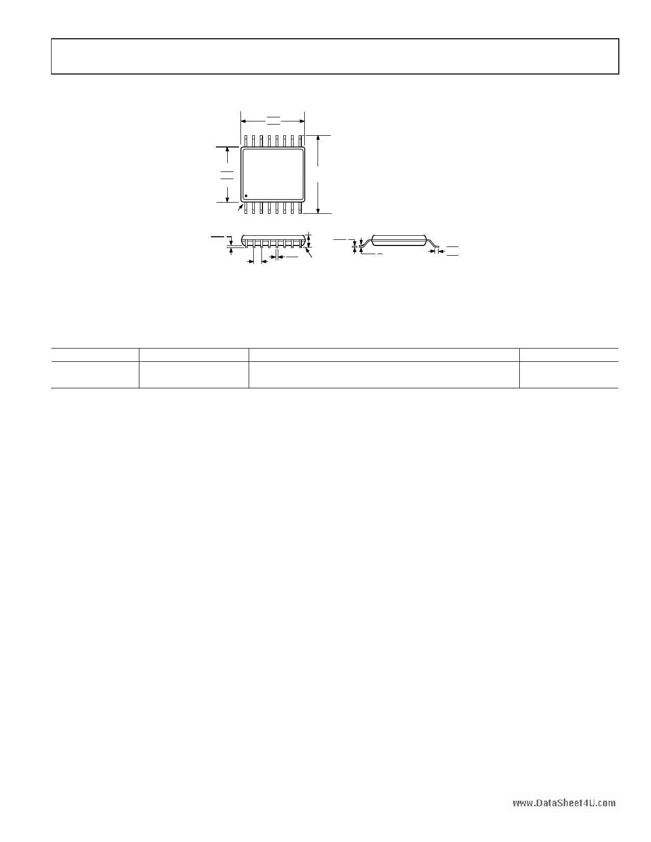
OUTLINE DIMENSIONS
5.10
5.00
4.90
16 9
4.50
4.40
4.30
6.40
BSC
18
PIN 1
0.15
0.05
1.20
MAX
0.20
0.09
0.65
BSC
0.30
0.19
COPLANARITY
0.10
SEATING
PLANE
8°
0°
0.75
0.60
0.45
COMPLIANT TO JEDEC STANDARDS MO-153-AB
Figure 15. 16-Lead Thin Shrink Small Outline Package [TSSOP]
(RU-16)
Dimensions shown in millimeters
ORDERING GUIDE
Model
Temperature Range
AD9573ARUZ1
−40°C to +85°C
AD9573-EVALZ1
Package Description
16-Lead Thin Shrink Small Outline Package [TSSOP]
Evaluation Board
1 Z = RoHS Compliant Part.
AD9573
Package Option
RU-16
Rev. 0 | Page 11 of 12
11 Page | ||
| Páginas | Total 12 Páginas | |
| PDF Descargar | [ Datasheet AD9573.PDF ] | |
Hoja de datos destacado
| Número de pieza | Descripción | Fabricantes |
| AD9571 | Ethernet Clock Generator | Analog Devices |
| AD9572 | Fiber Channel/Ethernet Clock Generator IC | Analog Devices |
| AD9573 | PCI-Express Clock Generator IC | Analog Devices |
| AD9574 | Ethernet/Gigabit Ethernet Clock Generator | Analog Devices |
| Número de pieza | Descripción | Fabricantes |
| SLA6805M | High Voltage 3 phase Motor Driver IC. |
Sanken |
| SDC1742 | 12- and 14-Bit Hybrid Synchro / Resolver-to-Digital Converters. |
Analog Devices |
|
DataSheet.es es una pagina web que funciona como un repositorio de manuales o hoja de datos de muchos de los productos más populares, |
| DataSheet.es | 2020 | Privacy Policy | Contacto | Buscar |
