|
|
|
PDF ADA4627-1 Data sheet ( Hoja de datos )
| Número de pieza | ADA4627-1 | |
| Descripción | JFET Operational Amplifier | |
| Fabricantes | Analog Devices | |
| Logotipo | ||
Hay una vista previa y un enlace de descarga de ADA4627-1 (archivo pdf) en la parte inferior de esta página. Total 20 Páginas | ||
|
No Preview Available !
Data Sheet
30 V, High Speed, Low Noise, Low Bias
Current, JFET Operational Amplifier
ADA4627-1/ADA4637-1
FEATURES
Low offset voltage: 200 μV maximum
Offset drift: 1 μV/°C typical
Very low input bias current: 5 pA maximum
Extended temperature range: −40°C to +125°C
±5 V to ±15 V dual supply
ADA4627-1 GBW: 19 MHz
ADA4637-1 GBW: 79 MHz
Voltage noise: 6.1 nV/√Hz at 1 kHz
ADA4627-1 slew rate: 82 V/μs
ADA4637-1 slew rate: 170 V/μs
High gain: 120 dB typical
High CMRR: 116 dB typical
High PSRR: 112 dB typical
APPLICATIONS
High impedance sensors
Photodiode amplifier
Precision instrumentation
Phase-locked loop filters
High end, professional audio
DAC output amplifier
ATE
Medical
GENERAL DESCRIPTION
The ADA4627-1/ADA4637-1 are wide bandwidth precision
amplifiers featuring low noise, very low offset, drift, and bias
current. The devices operate from ±5 V to ±15 V dual supply.
The ADA4627-1/ADA4637-1 provide benefits previously found
in few amplifiers. These amplifiers combine the best specifications
of precision dc and high speed ac op amps. The ADA4637-1 is
a decompensated version of the ADA4627-1 and is stable at a
noise gain of 5 or greater.
With a typical offset voltage of only 70 μV, drift of less than
1 μV/°C, and noise of only 0.86 μV p-p (0.1 Hz to 10 Hz), the
ADA4627-1/ADA4637-1 are suited for applications where error
sources cannot be tolerated.
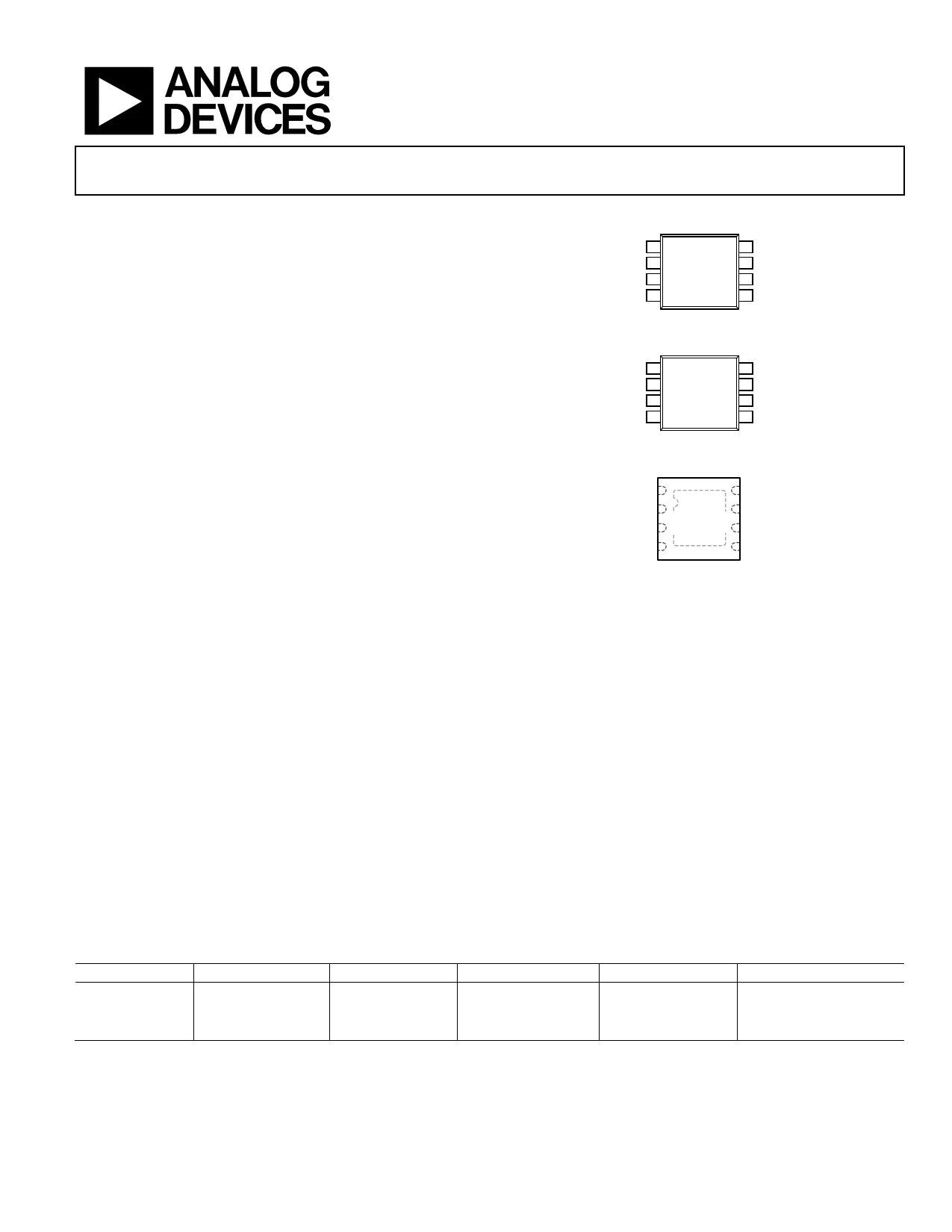
PIN CONFIGURATIONS
NULL 1
–IN 2
+IN 3
V– 4
8 NC
ADA4627-1 7 V+
TOP VIEW 6 OUT
(Not to Scale) 5 NULL
NC = NO CONNECT
Figure 1. 8-Lead SOIC_N (R-8)
NULL 1
–IN 2
+IN 3
V– 4
ADA4637-1
TOP VIEW
(Not to Scale)
8 NC
7 V+
6 OUT
5 NULL
NC = NO CONNECT
Figure 2. 8-Lead SOIC_N (R-8)
NC 1
–IN 2
+IN 3
V– 4
ADA4627-1/
ADA4637-1
TOP VIEW
8 NC
7 V+
6 OUT
5 NC
NOTES
1. NC = NO CONNECT.
2. IT IS RECOMMENDED
THAT THE EXPOSED PAD BE
CONNECTED TO V–.
Figure 3. 8-Lead LFCSP_VD (CP-8-13)
The ADA4627-1/ADA4637-1 are specified for both the
industrial temperature range of −25°C to +85°C and the
extended industrial temperature range of −40°C to +125°C. The
ADA4627-1/ADA4637-1 are available in tiny 8-lead LFCSP and
8-lead SOIC packages.
The ADA4627-1/ADA4637-1 are members of a growing series
of high speed, precision op amps offered by Analog Devices, Inc.
(see Table 1).
Table 1. High Speed Precision Op Amps
Supply
5 V Low Cost
5V
Single
AD8615
AD8651
Dual AD8616 AD8652
Quad
AD8618
26 V Low Power
AD8610
AD8620
30 V Low Cost
AD8510
AD8512
AD8513
30 V
ADA4627-1/ADA4637-1
Rev. F
Document Feedback
Information furnished by Analog Devices is believed to be accurate and reliable. However, no
responsibility is assumed by Analog Devices for its use, nor for any infringements of patents or other
rights of third parties that may result from its use. Specifications subject to change without notice. No
license is granted by implication or otherwise under any patent or patent rights of Analog Devices.
Trademarksandregisteredtrademarksarethepropertyoftheirrespectiveowners.
One Technology Way, P.O. Box 9106, Norwood, MA 02062-9106, U.S.A.
Tel: 781.329.4700 ©2009–2015 Analog Devices, Inc. All rights reserved.
Technical Support
www.analog.com
1 page 
Data Sheet
ABSOLUTE MAXIMUM RATINGS
Table 3.
Parameter
Supply Voltage
Input Voltage Range1
Input Current1
Differential Input Voltage2
Output Short-Circuit Duration to GND
Storage Temperature Range
Operating Temperature Range
Junction Temperature Range
Lead Temperature (Soldering, 60 sec)
ESD Human Body Model
Rating
36 V
(V−) − 0.3 V to (V+) + 0.3 V
±10 mA
±VSY
Indefinite
−65°C to +150°C
−40°C to +125°C
−65°C to +150°C
300°C
4 kV
1 Input pin has clamp diodes to the power supply pins. Input current should
be limited to 10 mA or less whenever input signals exceed the power supply
rail by 0.3 V.
2 Differential input voltage is limited to ±30 V or the supply voltage,
whichever is less.
Stresses at or above those listed under Absolute Maximum
Ratings may cause permanent damage to the product. This is a
stress rating only; functional operation of the product at these
or any other conditions above those indicated in the operational
section of this specification is not implied. Operation beyond
the maximum operating conditions for extended periods may
affect product reliability.
ADA4627-1/ADA4637-1
THERMAL RESISTANCE
θJA is specified for the worst-case conditions, that is, a device
soldered in a circuit board for surface-mount packages. This
was measured using a standard 2-layer board. For the LFCSP
package, the exposed pad should be soldered to a copper plane.
Table 4. Thermal Resistance
Package Type
8-Lead SOIC_N (R-8)
8-Lead LFCSP (CP-8-2)
θJA
155
77
θJC
45
14
Unit
°C/W
°C/W
ESD CAUTION
Rev. F | Page 5 of 20
5 Page 
Data Sheet
20
15
10
5
0
–5
–10
–15
–20
0
ADA4627-1
TA = 25°C
VSY = ±15V
VOUT
VIN
0.5 1.0 1.5 2.0 2.5 3.0 3.5 4.0
TIME (ms)
Figure 34. No Phase Reversal
1
VIN
2
VOUT
ADA4627-1
TA = 25°C
VSY = ±15
TIME (200ns/DIV)
Figure 35. Negative Settling Time to 0.01%
140
120
100
80
60
40
20
0 ADA4637-1
–20 VSY = ±15V
TA = 25ºC
–40 AV = –4
–60
RIN = 500Ω
RF = 2kΩ
–80
CF = 4.8pF
CL = 35pF
–100
10k 100k
GAIN
1M
FREQUENCY (Hz)
PHASE
10M 100M
Figure 36. Open-Loop Gain and Phase vs. Frequency
1
2 VOUT
VIN
ADA4627-1/ADA4637-1
ADA4627-1
TA = 25°C
VSY = ±15
TIME (200ns/DIV)
Figure 37. Positive Settling Time to 0.01%
1
ADA4627-1
TA = 25°C
VSY = ±15V
DUT GAIN = 100
4TH ORDER BAND PASS FIXTURE GAIN = 10k
TOTAL GAIN = 1M
TIME (1s/DIV)
Figure 38. 0.1 Hz to 10 Hz Noise
100
80
60
40
20
ADA4637-1
VTASY==25±º1C5V
0
10 100
1k 10k 100k 1M
FREQUENCY (Hz)
10M 100M
Figure 39. CMRR vs. Frequency
Rev. F | Page 11 of 20
11 Page | ||
| Páginas | Total 20 Páginas | |
| PDF Descargar | [ Datasheet ADA4627-1.PDF ] | |
Hoja de datos destacado
| Número de pieza | Descripción | Fabricantes |
| ADA4627-1 | JFET Operational Amplifier | Analog Devices |
| Número de pieza | Descripción | Fabricantes |
| SLA6805M | High Voltage 3 phase Motor Driver IC. |
Sanken |
| SDC1742 | 12- and 14-Bit Hybrid Synchro / Resolver-to-Digital Converters. |
Analog Devices |
|
DataSheet.es es una pagina web que funciona como un repositorio de manuales o hoja de datos de muchos de los productos más populares, |
| DataSheet.es | 2020 | Privacy Policy | Contacto | Buscar |