|
|
|
PDF ADAU1446 Data sheet ( Hoja de datos )
| Número de pieza | ADAU1446 | |
| Descripción | (ADAU1445 / ADAU1446) Digital Audio Processor | |
| Fabricantes | Analog Devices | |
| Logotipo | ||
Hay una vista previa y un enlace de descarga de ADAU1446 (archivo pdf) en la parte inferior de esta página. Total 70 Páginas | ||
|
No Preview Available !
www.DataSheet4U.com
SigmaDSP Digital Audio Processor
with Flexible Audio Routing Matrix
ADAU1445/ADAU1446
FEATURES
Fully programmable audio digital signal processor (DSP) for
enhanced sound processing
Features SigmaStudio, a proprietary graphical programming
tool for the development of custom signal flows
172 MHz SigmaDSP core; 3584 instructions per sample at 48 kHz
4k parameter RAM, 8k data RAM
Flexible audio routing matrix (FARM)
24-channel digital input and output
Up to 8 stereo asynchronous sample rate converters
(from 1:8 up to 7.75:1 ratio and 139 dB DNR)
Stereo S/PDIF input and output
Supports serial and TDM I/O, up to fS = 192 kHz
Multichannel byte-addressable TDM serial port
Pool of 170 ms digital audio delay (at 48 kHz)
Clock oscillator for generating master clock from crystal
PLL for generating core clock from common audio clocks
I2C and SPI control interfaces
Standalone operation
Self-boot from serial EEPROM
4-channel, 10-bit auxiliary control ADC
Multipurpose pins for digital controls and outputs
Easy implementation of available third-party algorithms
On-chip regulator for generating 1.8 V from 3.3 V supply
100-lead TQFP and LQFP packages
Temperature range: −40°C to +105°C
APPLICATIONS
Automotive audio processing
Head units
Navigation systems
Rear-seat entertainment systems
DSP amplifiers (sound system amplifiers)
Commercial audio processing
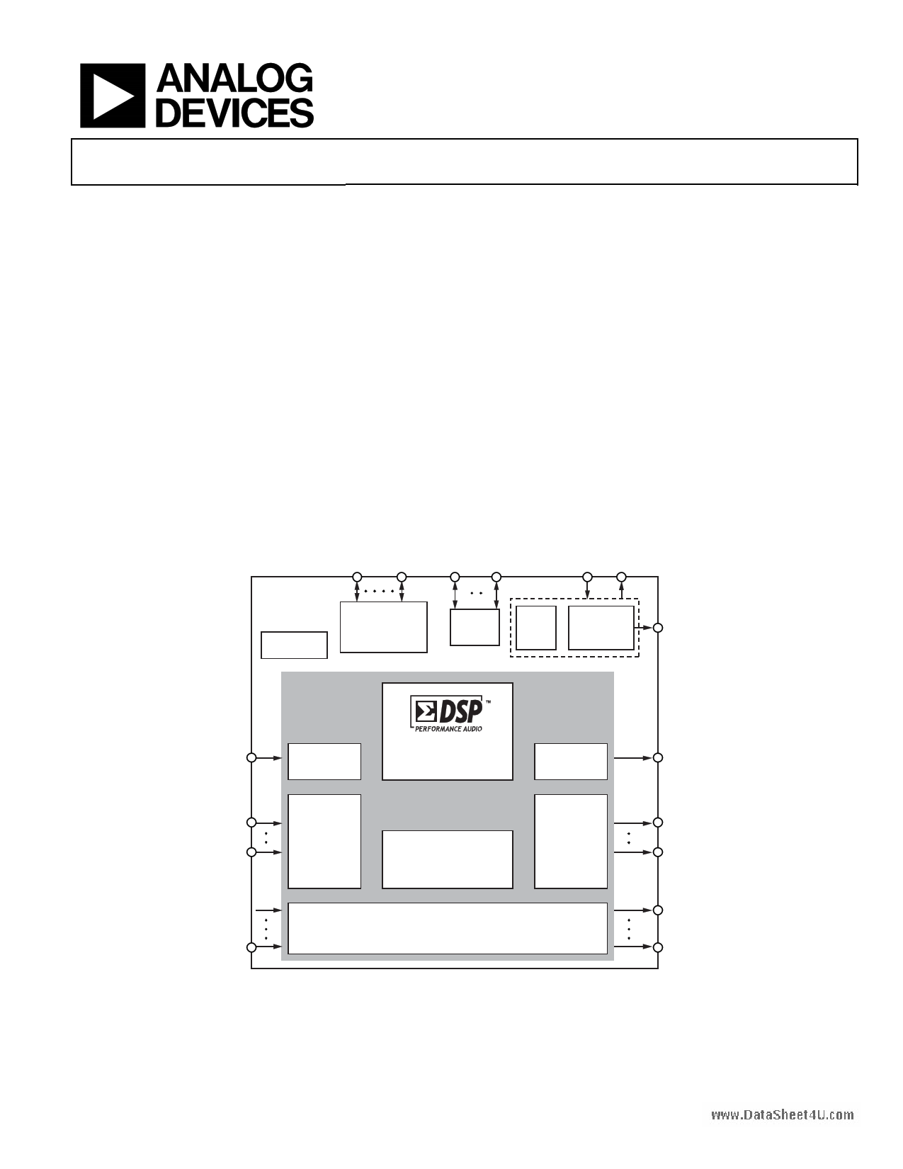
FUNCTIONAL BLOCK DIAGRAM
MP[3:0]/
SPI/I2C* SELFBOOT MP[11:4] ADC[3:0]
XTALI XTALO
ADAU1445/
ADAU1446
1.8V
REGULATOR
I2C/SPI CONTROL
INTERFACE
AND SELF-BOOT
MP/
AUX ADC
CLOCK
PLL OSCILLATOR
CLKOUT
SPDIFI
S/PDIF
RECEIVER
PROGRAMMABLE AUDIO
PROCESSOR CORE
S/PDIF
TRANSMITTER
SPDIFO
SDATA_IN[8:0]
(24-CHANNEL
DIGITAL AUDIO
INPUT)
BIT CLOCK†
(BCLK)
FRAME CLOCK†
(LRCLK)
FLEXIBLE AUDIO ROUTING MATRIX
(FARM)
SERIAL DATA
INPUT PORT
(×9)
UP TO 16 CHANNELS OF
ASYNCHRONOUS
SAMPLE RATE
CONVERTERS
SERIAL DATA
OUTPUT PORT
(×9)
SERIAL CLOCK
DOMAINS
(×12)
SDATA_OUT[8:0]
(24-CHANNEL
DIGITAL AUDIO
OUTPUT)
BIT CLOCK†
(BCLK)
FRAME CLOCK†
(LRCLK)
*SPI/I2C = THE ADDR0, CLATCH, SCL/CCLK, SDA/COUT, AND ADDR1/CDATA PINS.
†THERE ARE 12 BIT CLOCKS (BCLK[11:0]) AND 12 FRAME CLOCKS (LRCLK[11:0]) IN TOTAL. OF THE 12 CLOCKS,
SIX ARE ASSIGNABLE, THREE MUST BE OUTPUTS, AND THREE MUST BE INPUTS.
Figure 1.
Rev. A
Information furnished by Analog Devices is believed to be accurate and reliable. However, no
responsibility is assumed by Analog Devices for its use, nor for any infringements of patents or other
rights of third parties that may result from its use. Specifications subject to change without notice. No
license is granted by implication or otherwise under any patent or patent rights of Analog Devices.
Trademarksandregisteredtrademarksarethepropertyoftheirrespectiveowners.
One Technology Way, P.O. Box 9106, Norwood, MA 02062-9106, U.S.A.
Tel: 781.329.4700
www.analog.com
Fax: 781.461.3113
©2009 Analog Devices, Inc. All rights reserved.
1 page 
www.DataSheet4U.com
Parameter
Maximum Digital Current (DVDD) of
ADAU1445
Min
Typ Max
260 310
Minimum Digital Current (DVDD) of
ADAU1446
Maximum Digital Current (DVDD) of
ADAU1446
Power Dissipation
AVDD, DVDD, PVDD During Operation
of ADAU1445
AVDD, DVDD, PVDD During Operation
of ADAU1446
Reset, All Supplies
TEMPERATURE RANGE
Functionality Guaranteed
ASYNCHRONOUS SAMPLE RATE
CONVERTERS
Dynamic Range
I/O Sample Rate
I/O Sample Rate Ratio
THD + N
Group Delay
−40
6
1:8
100
195 235
640
500
94
+105
139
192
7.75:1
120 133
CRYSTAL OSCILLATOR
Transconductance
PLL
Lock Time
REGULATOR3
DVDD Voltage
40
10
1.65 1.75 1.85
1 SPDIFI input voltage range exceeds the requirements of the S/PDIF specification.
2 Maximum specifications are measured across −40°C to +105°C ambient.
3 Regulator specifications are calculated using an NJT4030P transistor from On Semiconductor in the circuit.
ADAU1445/ADAU1446
Unit Test Conditions/Comments
mA Full program loaded,
all serial ports active, all
ASRCs active.
mA Minimal program loaded,
one serial port active.
mA Full program loaded, all
serial ports active.
mW IOVDD is not included in
measurement.
mW IOVDD is not included in
measurement.
mW
°C Ambient.
dB A-weighted, 20 Hz to 20 kHz.
kHz
−dB
Refer to the SRC Group Delay
section.
mS
ms
V Maximum 500 mA load.
Rev. A | Page 5 of 92
5 Page 
www.DataSheet4U.com
ADAU1445/ADAU1446
Pin No.
6
Mnemonic
BCLK2
7 LRCLK2
8 SDATA_IN1
9 BCLK1
10 LRCLK1
11 SDATA_IN0
12 BCLK0
15 LRCLK0
16 MP11
17 MP10
18 MP9
19 MP8
20 ADDR0
Type1
D_IO
D_IO
D_IN
D_IO
D_IO
D_IN
D_IO
D_IO
D_IO
D_IO
D_IO
D_IO
D_IN
21 CLATCH D_IN
22
SCL/CCLK
D_IN
23
SDA/COUT
D_IO
24 ADDR1/CDATA D_IN
25, 37,
50, 75,
87, 100
28
DVDD
SELFBOOT
PWR
D_IN
29
CLKMODE1
D_IN
30
CLKMODE0
D_IN
31 RSVD
D_IN
32 PLL2
D_IN
33 MP7
D_IO
Description
Bit Clock, Input Clock Domain 2. This pin is bidirectional, with the direction depending on whether
the Input Clock Domain 2 is set up as a master or slave. When not used, this pin can be left disconnected.
Frame Clock, Input Clock Domain 2. This pin is bidirectional, with the direction depending on whether
the Input Clock Domain 2 is set up as a master or slave. When not used, this pin can be left disconnected.
Serial Data Port 1 Input. When not used, this pin can be left disconnected.
Bit Clock, Input Clock Domain 1. This pin is bidirectional, with the direction depending on whether
the Input Clock Domain 1 is set up as a master or slave. When not used, this pin can be left disconnected.
Frame Clock, Input Clock Domain 1. This pin is bidirectional, with the direction depending on whether
the Input Clock Domain 1 is set up as a master or slave. When not used, this pin can be left disconnected.
Serial Data Port 0 Input. When not used, this pin can be left disconnected.
Bit Clock, Input Clock Domain 0. This pin is bidirectional, with the direction depending on whether
the Input Clock Domain 0 is set up as a master or slave. When not used, this pin can be left disconnected.
Frame Clock, Input Clock Domain 0. This pin is bidirectional, with the direction depending on whether
the Input Clock Domain 0 is set up as a master or slave. When not used, this pin can be left disconnected.
Multipurpose, General-Purpose Input/Output. When not used, this pin can be left disconnected.
Multipurpose, General-Purpose Input/Output. When not used, this pin can be left disconnected.
Multipurpose, General-Purpose Input/Output. When not used, this pin can be left disconnected.
Multipurpose, General-Purpose Input/Output. When not used, this pin can be left disconnected.
Address 0 for I2C and SPI. In I2C mode, this pin, in combination with ADDR1, allows up to four
ADAU1445/ADAU1446 devices to be used on the same I2C bus. In SPI mode, setting ADDR0 either
low or high allows up to two ICs to be used with a common SPI latch signal.
SPI Latch Signal. Must go low at the beginning of an SPI transaction and high at the end of a
transaction. Each SPI transaction may take a different number of CCLK cycles to complete,
depending on the address and read/write bits that are sent at the beginning of the SPI transaction.
When not used, this pin should be tied to ground, preferably with a 10 kΩ pull-down resistor.
Serial Clock/Continuous Clock. In I2C mode, this pin functions as SCL and is always an open collector
input, except when in self-boot mode, where it is an open collector output (I2C master). The line
connected to this pin should have a 2.0 kΩ pull-up resistor. In SPI mode, this pin functions as CCLK
and is an input pin that can either run continuously or be gated off between SPI transactions.
Serial Data/Continuous Output. In I2C mode, this pin functions as SDA and is a bidirectional open
collector. The line connected to the SDA pin should have a 2.0 kΩ pull-up resistor. In SPI mode, this
pin functions as COUT and is used for reading back registers and memory locations. The COUT pin
is three-stated when an SPI read is not active.
Address 1/Continuous Data. In I2C mode, this pin functions as ADDR1 and, in combination with
ADDR0, sets the I2C address of the IC. This allows up to four ADAU1445/ADAU1446 devices to be
used on the same I2C bus. In SPI mode, this pin functions as CDATA and is the SPI data input.
1.8 V Digital Supply. This can be supplied externally or generated from a 3.3 V supply with the on-board
1.8 V regulator. Each DVDD pin should be decoupled to DGND with a 100 nF capacitor.
Self-Boot Select. Allows the ADAU1445/ADAU1446 to be controlled by the control port or to
perform a self-boot. Setting this pin high (that is, to 1) initiates a self-boot operation when the
ADAU1445/ADAU1446 are brought out of a reset. This pin can be tied directly to a voltage source
or ground or pulled up/down with a resistor.
Output Clock Mode 1. With CLKMODE0, this pin sets the frequency of the CLKOUT signal.
Output Clock Mode 0. With CLKMODE1, this pin sets the frequency of the CLKOUT signal.
Reserved. Tie this pin to ground, preferably with a 10 kΩ pull-down resistor.
PLL Mode Select Pin 2.
Multipurpose, General-Purpose Input/Output. When not used, this pin can be left disconnected.
Rev. A | Page 11 of 92
11 Page | ||
| Páginas | Total 70 Páginas | |
| PDF Descargar | [ Datasheet ADAU1446.PDF ] | |
Hoja de datos destacado
| Número de pieza | Descripción | Fabricantes |
| ADAU1442 | SigmaDSP Digital Audio Processor | Analog Devices |
| ADAU1445 | (ADAU1445 / ADAU1446) Digital Audio Processor | Analog Devices |
| ADAU1446 | (ADAU1445 / ADAU1446) Digital Audio Processor | Analog Devices |
| Número de pieza | Descripción | Fabricantes |
| SLA6805M | High Voltage 3 phase Motor Driver IC. |
Sanken |
| SDC1742 | 12- and 14-Bit Hybrid Synchro / Resolver-to-Digital Converters. |
Analog Devices |
|
DataSheet.es es una pagina web que funciona como un repositorio de manuales o hoja de datos de muchos de los productos más populares, |
| DataSheet.es | 2020 | Privacy Policy | Contacto | Buscar |