|
|
|
PDF ADG1613 Data sheet ( Hoja de datos )
| Número de pieza | ADG1613 | |
| Descripción | (ADG1611 - ADG1613) Quad SPST Switches | |
| Fabricantes | Analog Devices | |
| Logotipo | ||
Hay una vista previa y un enlace de descarga de ADG1613 (archivo pdf) en la parte inferior de esta página. Total 16 Páginas | ||
|
No Preview Available !
www.DataSheet4U.com
1 Ω Typical On Resistance, ±5 V, +12 V,
+5 V, and +3.3 V Quad SPST Switches
ADG1611/ADG1612/ADG1613
FEATURES
1 Ω typical on resistance
0.2 Ω on resistance flatness
±3.3 V to ±8 V dual supply operation
3.3 V to 16 V single supply operation
No VL supply required
3 V logic-compatible inputs
Rail-to-rail operation
Continuous current per channel
LFCSP package: 280 mA
TSSOP package: 175 mA
16-lead TSSOP and 16-lead, 4 mm × 4 mm LFCSP
APPLICATIONS
Communication systems
Medical systems
Audio signal routing
Video signal routing
Automatic test equipment
Data acquisition systems
Battery-powered systems
Sample-and-hold systems
Relay replacements
GENERAL DESCRIPTION
The ADG1611/ADG1612/ADG1613 contain four independent
single-pole/single-throw (SPST) switches. The ADG1611 and
ADG1612 differ only in that the digital control logic is inverted.
The ADG1611 switches are turned on with Logic 0 on the appro
priate control input, while Logic 1 is required for the ADG1612
switches. The ADG1613 has two switches with digital control
logic similar to that of the ADG1611; the logic is inverted on the
other two switches. Each switch conducts equally well in both
directions when on and has an input signal range that extends to
the supplies. In the off condition, signal levels up to the supplies
are blocked.
The ADG1613 exhibits break-before-make switching action for use
in multiplexer applications. Inherent in the design is low charge
injection for minimum transients when switching the digital inputs.
The ultralow on resistance of these switches make them ideal
solutions for data acquisition and gain switching applications
where low on resistance and distortion is critical. The on-resistance
profile is very flat over the full analog input range, ensuring
excellent linearity and low distortion when switching audio signals.
The CMOS construction ensures ultralow power dissipation, making
them ideally suited for portable and battery-powered instruments.
Rev. 0
Information furnished by Analog Devices is believed to be accurate and reliable. However, no
responsibility is assumed by Analog Devices for its use, nor for any infringements of patents or other
rights of third parties that may result from its use. Specifications subject to change without notice. No
license is granted by implication or otherwise under any patent or patent rights of Analog Devices.
Trademarksandregisteredtrademarksarethepropertyoftheirrespectiveowners.
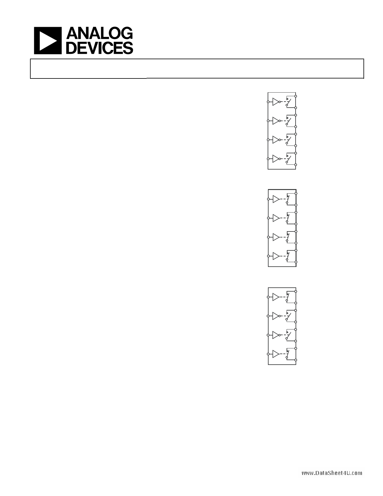
FUNCTIONAL BLOCK DIAGRAMS
IN1
IN2
ADG1611
IN3
IN4
S1
D1
S2
D2
S3
D3
S4
D4
NOTES
1. SWITCHES SHOWN FOR A LOGIC 1 INPUT.
Figure 1.
IN1
IN2
ADG1612
IN3
IN4
S1
D1
S2
D2
S3
D3
S4
D4
NOTES
1. SWITCHES SHOWN FOR A LOGIC 1 INPUT.
Figure 2.
S1
IN1
D1
S2
IN2
ADG1613
D2
S3
IN3
D3
S4
IN4
D4
NOTES
1. SWITCHES SHOWN FOR A LOGIC 1 INPUT.
Figure 3.
PRODUCT HIGHLIGHTS
1. 1.6 Ω maximum on resistance over temperature.
2. Minimum distortion: THD + N = 0.007%.
3. 3 V logic-compatible digital inputs: VINH = 2.0 V, VINL = 0.8 V.
4. No VL logic power supply required.
5. Ultralow power dissipation: <16 nW.
6. 16-lead TSSOP and 16-lead, 4 mm × 4 mm LFCSP.
One Technology Way, P.O. Box 9106, Norwood, MA 02062-9106, U.S.A.
Tel: 781.329.4700
www.analog.com
Fax: 781.461.3113
©2009 Analog Devices, Inc. All rights reserved.
1 page 
www.DataSheet4U.com
ADG1611/ADG1612/ADG1613
5 V SINGLE SUPPLY
VDD = 5 V ± 10%, VSS = 0 V, GND = 0 V, unless otherwise noted.
Table 3.
Parameter
ANALOG SWITCH
Analog Signal Range
On Resistance (RON)
On Resistance Match Between Channels (∆RON)
On Resistance Flatness (RFLAT(ON))
LEAKAGE CURRENTS
Source Off Leakage, IS (Off )
Drain Off Leakage, ID (Off )
Channel On Leakage, ID, IS (On)
DIGITAL INPUTS
Input High Voltage, VINH
Input Low Voltage, VINL
Input Current, IINL or IINH
Digital Input Capacitance, CIN
DYNAMIC CHARACTERISTICS1
tON
tOFF
Break-Before-Make Time Delay, tD (ADG1613 Only)
Charge Injection
Off Isolation
Channel-to-Channel Crosstalk
Total Harmonic Distortion + Noise
−3 dB Bandwidth
CS (Off )
CD (Off )
CD, CS (On)
POWER REQUIREMENTS
IDD
VDD
25°C
1.7
2.15
0.05
0.09
0.4
0.53
±0.05
±0.3
±0.05
±0.3
±0.15
±0.4
0.001
5
215
279
115
150
35
80
70
110
0.093
42
72
72
160
0.001
−40°C to
+85°C
2.4
0.12
0.55
±1
±1
±1.5
334
169
−40°C to
125°C
0 V to VDD
2.7
0.15
0.6
±6
±6
±10
2.0
0.8
±0.1
376
180
25
1
3.3/16
Unit
V
Ω typ
Ω max
Ω typ
Ω max
Ω typ
Ω max
nA typ
nA max
nA typ
nA max
nA typ
nA max
V min
V max
μA typ
μA max
pF typ
ns typ
ns max
ns typ
ns max
ns typ
ns min
pC typ
dB typ
dB typ
% typ
MHz typ
pF typ
pF typ
pF typ
μA typ
μA max
V min/max
Test Conditions/Comments
VS = 0 V to 4.5 V, IS = −10 mA; see Figure 24
VDD = 4.5 V, VSS = 0 V
VS = 0 V to 4.5 V, IS = −10 mA
VS = 0 V to 4.5 V, IS = −10 mA
VDD = 5.5 V, VSS = 0 V
VS = 1 V/4.5 V, VD = 4.5 V/1 V; see Figure 25
VS = 1 V/4.5 V, VD = 4.5 V/1 V; see Figure 25
VS = VD = 1 V or 4.5 V; see Figure 26
VIN = VGND or VDD
RL = 300 Ω, CL = 35 pF
VS = 2.5 V; see Figure 31
RL = 300 Ω, CL = 35 pF
VS = 2.5 V; see Figure 31
RL = 300 Ω, CL = 35 pF
VS1 = VS2 = 2.5 V; see Figure 32
VS = 0 V, RS = 0 Ω, CL = 1 nF; see Figure 33
RL = 50 Ω, CL = 5 pF, f = 100 kHz;
see Figure 27
RL = 50 Ω, CL = 5 pF, f = 100 kHz;
see Figure 28
RL = 110 Ω, f = 20 Hz to 20 kHz,
VS = 3.5 V p-p; see Figure 30
RL = 50 Ω, CL = 5 pF; see Figure 29
VS = 2.5 V, f = 1 MHz
VS = 2.5 V, f = 1 MHz
VS = 2.5 V, f = 1 MHz
VDD = 5.5 V
Digital inputs = 0 V or VDD
1 Guaranteed by design, not subject to production test.
Rev. 0 | Page 5 of 16
5 Page 
www.DataSheet4U.com
20
15
ID, IS (ON) +, +
10
ID (OFF) –, +
5 IS (OFF) +, –
0
–5 ID, IS (ON) –, –
IS (OFF) –, +
–10 ID (OFF) +, –
–15 0
20 40 60 80 100 120
TEMPERATURE (°C)
Figure 12. Leakage Currents as a Function of Temperature, ±5 V Dual Supply
25
20
15
10
5
0
–5
–10
–15
–20
0
ID, IS (ON) +, +
ID (OFF) –, +
IS (OFF) +, –
ID, IS (ON) –, –
IS (OFF) –, +
ID (OFF) +, –
20 40 60 80 100 120
TEMPERATURE (°C)
Figure 13. Leakage Currents as a Function of Temperature,
12 V Single Supply
20
15
ID, IS (OFF) +, +
10
ID, IS (OFF) –, –
5 ID (OFF) –, +
0
IS (OFF) +, –
IS (OFF) –, +
ID (OFF) +, –
–5
0 20 40 60 80 100 120
TEMPERATURE (°C)
Figure 14. Leakage Currents as a Function of Temperature,
5 V Single Supply
ADG1611/ADG1612/ADG1613
18
16
14
12 ID, IS (OFF) +, +
10
8 ID, IS (OFF) –, –
6 ID (OFF) –, +
4
IS (OFF) +, –
2
0
–2 IS (OFF) –, +
ID (OFF) +, –
–4
0 20 40 60 80 100 120
TEMPERATURE (°C)
Figure 15. Leakage Currents as a Function of Temperature,
3.3 V Single Supply
600
500
IIDSSD
=
=
+12V
0V
400
IDD PER CHANNEL
TA = 25°C
300
200
100
0
–100
0
IIDSSD
=
=
+5V
–5V
IIDSSD
=
=
+5V
0V
IIDSSD
=
=
+3.3V
0V
246
LOGIC (V)
8
10 12
Figure 16. IDD vs. Logic Level
300
250
VVDSSD
=
=
+5V
–5V
200
150
VVDSSD
=
=
+12V
0V
100
50
0
–6 –4 –2
0
VVDSSD
=
=
+5V
0V
VVDSSD
=
=
+3.3V
0V
2 4 6 8 10 12 14
VS (V)
Figure 17. Charge Injection vs. Source Voltage
Rev. 0 | Page 11 of 16
11 Page | ||
| Páginas | Total 16 Páginas | |
| PDF Descargar | [ Datasheet ADG1613.PDF ] | |
Hoja de datos destacado
| Número de pieza | Descripción | Fabricantes |
| ADG1611 | (ADG1611 - ADG1613) Quad SPST Switches | Analog Devices |
| ADG1612 | (ADG1611 - ADG1613) Quad SPST Switches | Analog Devices |
| ADG1613 | (ADG1611 - ADG1613) Quad SPST Switches | Analog Devices |
| Número de pieza | Descripción | Fabricantes |
| SLA6805M | High Voltage 3 phase Motor Driver IC. |
Sanken |
| SDC1742 | 12- and 14-Bit Hybrid Synchro / Resolver-to-Digital Converters. |
Analog Devices |
|
DataSheet.es es una pagina web que funciona como un repositorio de manuales o hoja de datos de muchos de los productos más populares, |
| DataSheet.es | 2020 | Privacy Policy | Contacto | Buscar |