|
|
|
PDF MAX3627 Data sheet ( Hoja de datos )
| Número de pieza | MAX3627 | |
| Descripción | Precision Clock Generator | |
| Fabricantes | Maxim Integrated Products | |
| Logotipo | ||
Hay una vista previa y un enlace de descarga de MAX3627 (archivo pdf) en la parte inferior de esta página. Total 11 Páginas | ||
|
No Preview Available !
19-4567; Rev 0; 4/09
www.DataSheet4U.com
EVAALVUAAILTAIOBNLEKIT
+3.3V, Low-Jitter, Precision Clock
Generator with Multiple Outputs
General Description
The MAX3627 is a low-jitter, precision clock generator
optimized for network applications. The device inte-
grates a crystal oscillator and a phase-locked loop
(PLL) to generate high-frequency clock outputs for
Ethernet applications.
Maxim’s proprietary PLL design features ultra-low jitter
(0.4psRMS) and excellent power-supply noise rejection
(PSNR), minimizing design risk for network equipment.
The MAX3627 contains seven LVDS outputs and one
LVCMOS output. The output frequencies are selectable
among 125MHz, 156.25MHz, and 312.5MHz.
Applications
Ethernet Networking Equipment
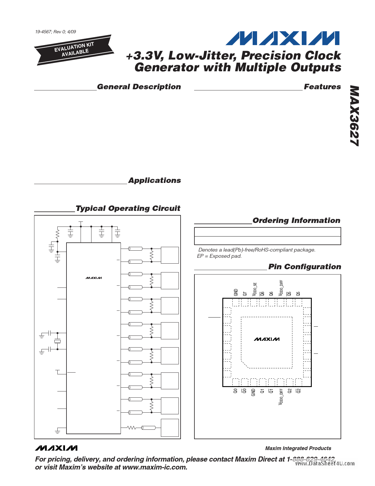
Typical Operating Circuit
+3.3V ±5%
10.5Ω
0.1μF
0.1μF
0.1μF
10μF
0.01μF
VDDA
VDD VDDO_DIFF
OPEN
OPEN
OSC_IN
OE
MAX3627
33pF
25MHz
(CL = 18pF)
27pF
X_OUT
X_IN
VDD
PLL_BP
GND, OPEN, OR VDD
FSELA
GND, OPEN, OR VDD
FSELB
VDDO_SE 125MHz/156MHz/312.5MHz
Q0 Z0 = 50Ω
100Ω
Q0 Z0 = 50Ω
125MHz/156MHz/312.5MHz
Q1 Z0 = 50Ω
100Ω
Q1 Z0 = 50Ω
125MHz/156MHz/312.5MHz
Q2 Z0 = 50Ω
100Ω
Q2 Z0 = 50Ω
125MHz/156MHz/312.5MHz
Q3 Z0 = 50Ω
100Ω
Q3 Z0 = 50Ω
125MHz/156MHz/312.5MHz
Q4 Z0 = 50Ω
100Ω
Q4 Z0 = 50Ω
125MHz/156MHz/312.5MHz
Q5 Z0 = 50Ω
100Ω
Q5 Z0 = 50Ω
125MHz/156MHz/312.5MHz
Q6 Z0 = 50Ω
100Ω
Q6 Z0 = 50Ω
ASIC
ASIC
ASIC
ASIC
ASIC
ASIC
ASIC
33Ω 125MHz/156.25MHz
GND
Q7
Z0 = 50Ω
ASIC
Features
♦ Crystal Oscillator Interface: 25MHz
♦ OSC_IN Interface
PLL Enabled: 25MHz
PLL Disabled: 20MHz to 320MHz
♦ Outputs
One LVDS Output at 125MHz/156.25MHz/
312.5MHz (Selectable with FSELA)
Six LVDS Outputs at 125MHz/156.25MHz/
312.5MHz (Selectable with FSELB)
One LVCMOS Output at 125MHz/156.25MHz
(Selectable with FSELB)
♦ Low Phase Jitter
0.4psRMS (12kHz to 20MHz)
0.2psRMS (1.875MHz to 20MHz)
♦ Excellent PSNR: -64dBc at 156.25MHz with
40mVP-P Supply Noise at 100kHz
♦ Operating Temperature Range: 0°C to +70°C
Ordering Information
PART
TEMP RANGE
PIN-PACKAGE
MAX3627CTJ+
0°C to +70°C
32 TQFN-EP*
+Denotes a lead(Pb)-free/RoHS-compliant package.
*EP = Exposed pad.
Pin Configuration
TOP VIEW
24 23 22 21 20 19 18 17
VDD 25
16 OE
PLL_BP 26
15 FSELB
VDDA 27
14 Q4
FSELA 28
OSC_IN 29
MAX3627
13 Q4
12 VDDO_DIFF
X_IN 30
11 Q3
X_OUT 31
GND 32
+
*EP 10 Q3
9 GND
1 2345678
THIN QFN
(5mm × 5mm)
*EXPOSED PAD CONNECTED TO GROUND.
________________________________________________________________ Maxim Integrated Products 1
For pricing, delivery, and ordering information, please contact Maxim Direct at 1-888-629-4642,
or visit Maxim’s website at www.maxim-ic.com.
1 page 
www.DataSheet4U.com
+3.3V, Low-Jitter, Precision Clock
Generator with Multiple Outputs
MAX3627
Q7
33Ω
Z0 = 50Ω
VCC
800Ω
3pF
800Ω
0.1μF
50Ω
Z0 = 50Ω
OSCILLOSCOPE
50Ω
Figure 2. LVCMOS Output Measurement Setup
Typical Operating Characteristics
(Typical values are at VDD = +3.3V, TA = +25°C, crystal frequency = 25MHz.)
300
275
250
225
200
175
150
125
100
75
50
25
0
0
SUPPLY CURRENT
vs. TEMPERATURE
PLL_BP = HIGH
PLL_BP = LOW
10 20 30 40 50 60 70
AMBIENT TEMPERATURE (°C)
-80
-90
-100
-110
-120
-130
-140
-150
-160
0.1
PHASE NOISE AT 125MHz
CLOCK FREQUENCY (Q0)
1 10 100 1000 10,000 100,000
OFFSET FREQUENCY (kHz)
-80
-90
-100
-110
-120
-130
-140
-150
-160
0.1
PHASE NOISE AT 125MHz
CLOCK FREQUENCY (Q7)
1 10 100 1000 10,000 100,000
OFFSET FREQUENCY (kHz)
_______________________________________________________________________________________ 5
5 Page 
www.DataSheet4U.com
+3.3V, Low-Jitter, Precision Clock
Generator with Multiple Outputs
Interface Models
Figures 7, 8, and 9 show examples of interface models.
OSC_IN
VDD 1.4V
180kΩ
ESD
STRUCTURES
Figure 7. Simplified OSC_IN Pin Circuit Schematic
VDDO_SE
10Ω
Q7
10Ω
ESD
STRUCTURES
Figure 8. Simplified LVCMOS Output Circuit Schematic
VDDO_DIFF VDD
75kΩ
OE
ESD
STRUCTURES
Figure 9. Simplified OE Pin Circuit Schematic
Layout Considerations
The inputs and outputs are the most critical paths for
the MAX3627 and great care should be taken to mini-
mize discontinuities on these transmission lines
between the connector and the IC. Here are some sug-
gestions for maximizing the performance of the
MAX3627:
• An uninterrupted ground plane should be posi-
tioned beneath the clock outputs. The ground
plane under the crystal should be removed to mini-
mize capacitance.
• Ground pin vias should be placed close to the IC
and the input/output interfaces to allow a return
current path to the MAX3627 and the receive
devices.
• Supply decoupling capacitors should be placed
close to the supply pins, preferably on the same
layer as the MAX3627.
• Take care to isolate crystal input traces from the
MAX3627 outputs.
• The crystal, trace, and two external capacitors
should be placed on the board as close as possi-
ble to the X_IN and X_OUT pins.
• Maintain 100Ω differential (or 50Ω single-ended)
transmission line impedance into and out of the part.
• Use good high-frequency layout techniques and
multilayer boards with an uninterrupted ground
plane to minimize EMI and crosstalk.
Refer to the MAX3627 evaluation kit for more information.
Exposed-Pad Package
The exposed pad on the 32-pin TQFN package pro-
vides a very low inductance path for return current trav-
eling to the PCB ground plane. The pad is thermal and
electrical ground on the MAX3627 and must be sol-
dered to the circuit board ground for proper electrical
performance.
Chip Information
PROCESS: BiCMOS
Package Information
For the latest package outline information and land patterns, go
to www.maxim-ic.com/packages.
PACKAGE TYPE PACKAGE CODE DOCUMENT NO.
32 TQFN-EP
T3255+5
21-0140
Maxim cannot assume responsibility for use of any circuitry other than circuitry entirely embodied in a Maxim product. No circuit patent licenses are
implied. Maxim reserves the right to change the circuitry and specifications without notice at any time.
Maxim Integrated Products, 120 San Gabriel Drive, Sunnyvale, CA 94086 408-737-7600 ____________________ 11
© 2009 Maxim Integrated Products
Maxim is a registered trademark of Maxim Integrated Products, Inc.
11 Page | ||
| Páginas | Total 11 Páginas | |
| PDF Descargar | [ Datasheet MAX3627.PDF ] | |
Hoja de datos destacado
| Número de pieza | Descripción | Fabricantes |
| MAX3620 | Delay Lines | Maxim Integrated Products |
| MAX3622 | Precision Clock Generator | Maxim Integrated Products |
| MAX3624 | Precision Clock Generator | Maxim Integrated Products |
| MAX3624A | Precision Clock Generator | Maxim Integrated Products |
| Número de pieza | Descripción | Fabricantes |
| SLA6805M | High Voltage 3 phase Motor Driver IC. |
Sanken |
| SDC1742 | 12- and 14-Bit Hybrid Synchro / Resolver-to-Digital Converters. |
Analog Devices |
|
DataSheet.es es una pagina web que funciona como un repositorio de manuales o hoja de datos de muchos de los productos más populares, |
| DataSheet.es | 2020 | Privacy Policy | Contacto | Buscar |