|
|
|
PDF LTC6420-20 Data sheet ( Hoja de datos )
| Número de pieza | LTC6420-20 | |
| Descripción | Dual Matched 1.8GHz Differential Amplifier/ADC Drivers | |
| Fabricantes | Linear Technology | |
| Logotipo | ||
Hay una vista previa y un enlace de descarga de LTC6420-20 (archivo pdf) en la parte inferior de esta página. Total 12 Páginas | ||
|
No Preview Available !
www.DataSheet4U.com
FEATURES
n Matched Gain ±0.1dB
n Matched Phase ±0.1° at 100MHz
n Channel Separation 80dB at 100MHz
n 1.8GHz –3dB Bandwidth; Fixed Gain of 10V/V (20dB)
n IMD3 = –84dBc at 100MHz, 2VP-P
n Equivalent OIP3 = 46dBm at 100MHz
n 1nV/√Hz Internal Op Amp Noise
n 6.2dB Noise Figure
n Differential Inputs and Outputs
n Rail-to-Rail Output Swing
n 80mA Supply Current (240mW) per Amplifier
n 1.1V to 1.6V Output Common Mode Voltage,
Adjustable
n DC- or AC-Coupled Operation
n 20-Lead 3mm × 4mm × 0.75mm QFN Package
APPLICATIONS
n Differential ADC Driver
n Differential Driver/Receiver
n Single Ended to Differential Conversion
n IF Sampling (Diversity) Receivers
LTC6420-20
Dual Matched
1.8GHz Differential
Amplifiers/ADC Drivers
DESCRIPTION
The LTC®6420-20 is a dual high-speed differential amplifier
targeted at processing signals from DC to 300MHz. The
part has been specifically designed to drive 12-, 14- and
16-bit ADCs with low noise and low distortion, but can also
be used as a general-purpose broadband gain block.
The LTC6420-20 is easy to use, with minimal support
circuitry required. The output common mode voltage
is set using an external pin, independent of the inputs,
which eliminates the need for transformers or AC-coupling
capacitors in many applications. The gain is internally
fixed at 20dB (10V/V).
The LTC6420-20 saves space and power compared to
alternative solutions using IF gain blocks and transformers.
The LTC6420-20 is packaged in a compact 20-lead
3mm × 4mm QFN package and operates over the –40°C
to 85°C temperature range.
L, LT, LTC and LTM are registered trademarks of Linear Technology Corporation.
All other trademarks are the property of their respective owners.
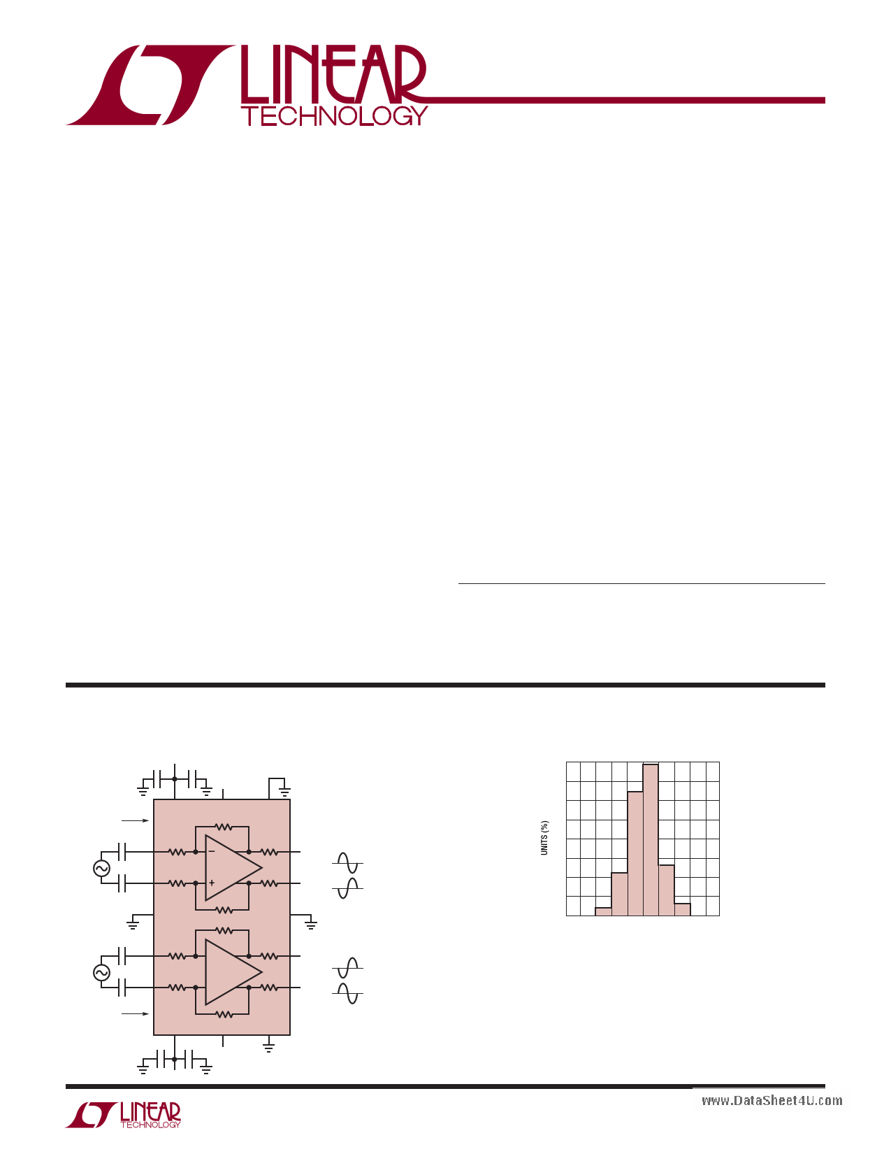
TYPICAL APPLICATION
Matched Dual Amplifier with Output Common Mode Biasing
3V
0.1μF 1000pF
VOCM A
VIN A
VIN B
ZIN = 200Ω
V+ A
0.1μF
–IN A
100Ω
0.1μF
+IN A
100Ω
VOCM A
1000Ω
–
+
1000Ω
V–
LTC6420-20 1000Ω
0.1μF
+IN B
0.1μF
–IN B
100Ω
100Ω
+
–
1000Ω
ZIN = 200Ω
V+ B
VOCM B
0.1μF 1000pF VOCM B
ENABLEA
12.5Ω
12.5Ω
12.5Ω
12.5Ω
ENABLEB
+OUT A
VOCM A
–OUT A
VOCM A
V–
±0.1dB GAIN MATCHING
±0.1° PHASE MATCHING AT 100MHz
– OUT B
+OUT B
VOCM B
VOCM B
642020 TA01a
3V
Distribution of Gain Match
40
35
30
25
20
15
10
5
0
– 0.25 – 0.15 – 0.05 0.05 0.15 0.25
CHANNEL-TO-CHANNEL GAIN MATCH (dB)
642020 TA01b
642020fa
1
1 page 
www.DataSheet4U.com
TYPICAL PERFORMANCE CHARACTERISTICS
LTC6420-20
Channel to Channel Gain Match
vs Frequency
0.5
0.4
0.3
0.2
0.1
0.0
–0.1
–0.2
–0.3
–0.4
–0.5
10
100
FREQUENCY (MHz)
1000 2000
642020 G01
Channel to Channel Group Delay
Match vs Frequency
0.5
0.4
0.3
0.2
0.1
0.0
–0.1
–0.2
–0.3
–0.4
–0.5
10
100
FREQUENCY (MHz)
1000 2000
642020 G02
Channel to Channel Phase Match
vs Frequency
0.5
0.4
0.3
0.2
0.1
0.0
–0.1
–0.2
–0.3
–0.4
–0.5
10
100
FREQUENCY (MHz)
1000
642020 G03
Frequency Response
25 TEST CIRCUIT B
20
15
10
5
0
10 100 1000 3000
FREQUENCY (MHz)
642020 G04
Input and Output Reflection and
Reverse Isolation vs Frequency
0
TEST CIRCUIT B
–10
–20 S11
–30
–40 S22
–50
–60 S12
–70
–80
10
100 1000 3000
FREQUENCY (MHz)
642020 G06
S21 Phase and Group Delay
vs Frequency
0 TEST CIRCUIT B 1.2
–100
0.9
–200
0.6
–300
–400
0
0.3
PHASE
GROUP DELAY
200 400 600
FREQUENCY (MHz)
0
800 1000
642020 G05
Input and Output Impedance
vs Frequency
250
50
ZIN
200
ZOUT
150
ZIN
100
PHASE
IMPEDANCE MAGNITUDE
50
30
10
–10
–30
ZOUT
0 –50
1 10 100 1000
FREQUENCY (MHz)
642020 G07
642020fa
5
5 Page 
www.DataSheet4U.com
TYPICAL APPLICATIONS
Test Circuit B, 4-Port Measurements
(Only the Signal-Path Connections Are Shown)
0.1μF
PORT 1
(50Ω)
+INA
1/2
AGILENT
E5071C
200Ω
0.1μF
PORT 2
(50Ω)
–INA
RG
100Ω
RG
100Ω
RF
1000Ω
– ++
++ ––
RF
1000Ω
ROUT
12.5Ω
ROUT
12.5Ω
+OUTA 37.4Ω 0.1μF
–OUTA 37.4Ω
0.1μF
PORT 3
(50Ω)
1/2 AGILENT
E5071C
PORT 4
(50Ω)
642020 TA02
(B CHANNEL NOT SHOWN)
LTC6420-20
Parallel ADC Drivers to Reduce Wideband Noise
3.3V 3.3V
C1
0.1μF
+– VIN
1/2
LTC6420-20
R5
49.9Ω
R6
49.9Ω
1/2
LTC6420-20
VOCM
R7
49.9Ω
R8
49.9Ω
C4
0.1μF
C2 R3
12pF 10Ω
C5 R4
12pF 10Ω
C3
12pF
LTC2208
VCM
–3dB FILTER BANDWIDTH = 120MHz
C6
2.2μF
642020 TA03
PACKAGE DESCRIPTION
UDC Package
20-Lead Plastic QFN (3mm × 4mm)
(Reference LTC DWG # 05-08-1742 Rev Ø)
3.50 ± 0.05
2.10 ± 0.05
1.50 REF
2.65 ± 0.05
1.65 ± 0.05
0.70 ±0.05
3.00 ± 0.10
4.00 ± 0.10
PACKAGE
OUTLINE
PIN 1
TOP MARK
(NOTE 6)
0.75 ± 0.05
R = 0.05 TYP
2.50 REF
1.50 REF
19 20
2.65 ± 0.10
1.65 ± 0.10
PIN 1 NOTCH
R = 0.20 OR 0.25
× 45° CHAMFER
0.40 ± 0.10
1
2
0.25 ±0.05
0.50 BSC
2.50 REF
3.10 ± 0.05
4.50 ± 0.05
RECOMMENDED SOLDER PAD PITCH AND DIMENSIONS
APPLY SOLDER MASK TO AREAS THAT ARE NOT SOLDERED
0.200 REF
0.00 – 0.05
(UDC20) QFN 1106 REV Ø
R = 0.115
TYP
0.25 ± 0.05
0.50 BSC
BOTTOM VIEW—EXPOSED PAD
NOTE:
1. DRAWING IS NOT A JEDEC PACKAGE OUTLINE
2. DRAWING NOT TO SCALE
3. ALL DIMENSIONS ARE IN MILLIMETERS
4. DIMENSIONS OF EXPOSED PAD ON BOTTOM OF PACKAGE DO NOT INCLUDE
MOLD FLASH. MOLD FLASH, IF PRESENT, SHALL NOT EXCEED 0.15mm ON ANY SIDE
5. EXPOSED PAD SHALL BE SOLDER PLATED
6. SHADED AREA IS ONLY A REFERENCE FOR PIN 1 LOCATION
ON THE TOP AND BOTTOM OF PACKAGE
Information furnished by Linear Technology Corporation is believed to be accurate and reliable.
However, no responsibility is assumed for its use. Linear Technology Corporation makes no representa-
tion that the interconnection of its circuits as described herein will not infringe on existing patent rights.
642020fa
11
11 Page | ||
| Páginas | Total 12 Páginas | |
| PDF Descargar | [ Datasheet LTC6420-20.PDF ] | |
Hoja de datos destacado
| Número de pieza | Descripción | Fabricantes |
| LTC6420-20 | Dual Matched 1.8GHz Differential Amplifier/ADC Drivers | Linear Technology |
| Número de pieza | Descripción | Fabricantes |
| SLA6805M | High Voltage 3 phase Motor Driver IC. |
Sanken |
| SDC1742 | 12- and 14-Bit Hybrid Synchro / Resolver-to-Digital Converters. |
Analog Devices |
|
DataSheet.es es una pagina web que funciona como un repositorio de manuales o hoja de datos de muchos de los productos más populares, |
| DataSheet.es | 2020 | Privacy Policy | Contacto | Buscar |