|
|
|
PDF LTM4608 Data sheet ( Hoja de datos )
| Número de pieza | LTM4608 | |
| Descripción | 8A DC/DC uModule | |
| Fabricantes | Linear Technology | |
| Logotipo | ||
Hay una vista previa y un enlace de descarga de LTM4608 (archivo pdf) en la parte inferior de esta página. Total 24 Páginas | ||
|
No Preview Available !
www.DataSheet4U.com
LTM4608
Low VIN, 8A DC/DC
µModuleTM with Tracking, Margining,
and Frequency Synchronization
FEATURES
■ Complete Standalone Power Supply
■ ±1.5% Output Voltage Regulation
■ 2.375V to 5.5V Input Voltage Range
■ 8A DC, 10A Peak Output Current
■ 0.6V Up to 5V Output
■ Output Voltage Tracking and Margining
■ Power Good Tracks Margining
■ Multiphase Operation
■ Parallel Current Sharing
■ Onboard Frequency Synchronization
■ Spread Spectrum Frequency Modulation
■ Overcurrent/Thermal Shutdown Protection
■ Current Mode Control/Fast Transient Response
■ Selectable Burst Mode® Operation
■ Up to 95% Efficiency
■ Output Overvoltage Protection
■ Small Surface Mount Footprint, Low Profile
(15mm × 9mm × 2.8mm) LGA Package
APPLICATIONS
■ Telecom, Networking and Industrial Equipment
■ Storage Systems
■ Point of Load Regulation
DESCRIPTION
The LTM®4608 is a complete 8A switch mode DC/DC power
supply. Included in the package are the switching control-
ler, power FETs, inductor and all support components.
Operating over an input voltage range of 2.375V to 5.5V,
the LTM4608 supports an output voltage range of 0.6V
to 5V, set by a single external resistor. This high efficiency
design delivers up to 8A continuous current (10A peak).
Only bulk input and output capacitors are needed.
The low profile package (2.8mm) enables utilization of
unused space on the back side of PC boards for high
density point-of-load regulation. The high switching
frequency and a current mode architecture enable a very
fast transient response to line and load changes without
sacrificing stability. The device supports frequency syn-
chronization, programmable multiphase and/or spread
spectrum operation, output voltage tracking for supply
rail sequencing and voltage margining.
Fault protection features include overvoltage protection,
overcurrent protection and thermal shutdown. The power
module is offered in a compact and thermally enhanced
15mm × 9mm × 2.8mm LGA package. The LTM4608 is
Pb-free and RoHS compliant .
, LT, LTC, LTM and Burst Mode are registered trademarks of Linear Technology
Corporation. μModule is a trademark of Linear Technology Corporation.
All other trademarks are the property of their respective owners.
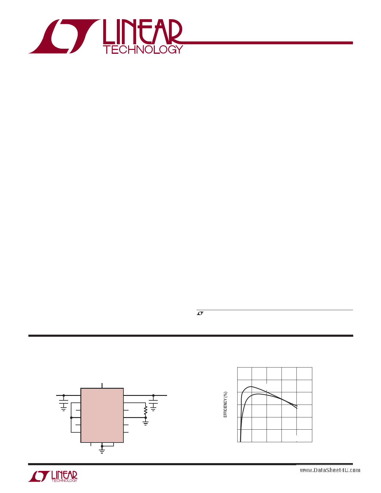
TYPICAL APPLICATION
3V to 5.5V Input to 1.8V Output DC/DC μModule
CLKIN
VIN
3V TO 5.5V
10μF
CLKIN
VIN VOUT
SVIN
FB
SW ITH
RUN LTM4608 ITHM
PLLLPF
PGOOD
4.87k
PGOOD
TRACK
MGN VOUT
CLKOUT GND SGND
4608 TA01a
VOUT
1.8V
100μF
Efficiency vs Load Current
100
95
VIN = 3.3V
90
VIN = 5V
85
80
75
70
0
VOUT = 1.8V
2 4 6 8 10
LOAD CURRENT (A)
4608 TA01b
4608f
1
1 page 
www.DataSheet4U.com
LTM4608
TYPICAL PERFORMANCE CHARACTERISTICS per Figure 18 Typcial Application
Efficiency vs Load Current
100
CONTINUOUS MODE
95
Efficiency vs Load Current
100
CONTINUOUS MODE
95
90 90
85 85
80
75
70
0
5VIN 1.2VOUT
5VIN 1.5VOUT
5VIN 1.8VOUT
5VIN 2.5VOUT
5VIN 3.3VOUT
24 6
LOAD CURRENT
8
4608 G01
80
75
70
0
3.3VIN 1.2VOUT
3.3VIN 1.5VOUT
3.3VIN 1.8VOUT
3.3VIN 2.5VOUT
246
LOAD CURRENT
8
4608 G02
Burst Mode Efficiency with
5V Input
100
90
80
70
60
50 VOUT = 1.5V
VOUT = 2.5V
VOUT = 3.3V
40
0 0.1 0.2 0.3 0.4 0.5 0.6 0.7 0.8 0.9 1.0 1.1
LOAD CURRENT (A)
4608 G04
VIN to VOUT Step-Down Ratio
4.0
IOUT = 8A
3.5 VOUT = 1.2V
VOUT = 1.5V
3.0 VOUT = 1.8V
VOUT = 2.5V
2.5 VOUT = 3.3V
2.0
1.5
1.0
0.5
0
0123456
VIN (V)
4608 G05
Supply Current vs VIN
1.6
1.4
1.2 VO = 1.2V PULSE-SKIPPING MODE
1
0.8
0.6 VO = 1.2V BURST MODE
0.4
0.2
0
2.5
3 3.5 4 4.5
INPUT VOLTAGE (V)
5 5.5
4608 G07
Load Transient Response
1A/DIV
20mV/DIV
VIN = 5V
VOUT = 3.3V
2A/μs STEP
20μs/DIV
4608 G08
COUT = 100μF X5R
C1 = 100pF, C3 = 22pF FROM FIGURE 18
Efficiency vs Load Current
100
CONTINUOUS MODE
95
90
85
80
75
70
01
2.5VIN 1.0VOUT
2.5VIN 1.5VOUT
2.5VIN 1.8VOUT
2 34 5
LOAD CURRENT (A)
67
4608 G03
VIN to VOUT Step-Down Ratio
4.0
IOUT = 5A
3.5 VOUT = 1.2V
VOUT = 1.5V
3.0 VOUT = 1.8V
VOUT = 2.5V
2.5 VOUT = 3.3V
2.0
1.5
1.0
0.5
0
0123456
VIN (V)
4608 G06
Load Transient Response
2A/DIV
20mV/DIV
VIN = 5V
VOUT = 2.5V
2.5A/μs STEP
20μs/DIV
4608 G09
COUT = 100μF X5R
C1 = 120pF, C3 = 47pF FROM FIGURE 18
4608f
5
5 Page 
www.DataSheet4U.com
LTM4608
APPLICATIONS INFORMATION
D = VOUT
VIN
Without considering the inductor current ripple, the RMS
current of the input capacitor can be estimated as:
( )ICIN(RMS)
=
IOUT(MAX )
η%
•
D • 1– D
In the above equation, η% is the estimated efficiency of
the power module. The bulk capacitor can be a switcher-
rated electrolytic aluminum capacitor, polymer capacitor
for bulk input capacitance due to high inductance traces
or leads. If a low inductance plane is used to power the
device, then only one 10μF ceramic is required. The three
internal 10μF ceramics are typically rated for 2A of RMS
ripple current, so the ripple current at the worse case for
8A maximum current is 4A or less.
Output Capacitors
The LTM4608 is designed for low output voltage ripple
noise. The bulk output capacitors defined as COUT are
chosen with low enough effective series resistance (ESR)
to meet the output voltage ripple and transient require-
ments. COUT can be a low ESR tantalum capacitor, a low
ESR polymer capacitor or ceramic capacitor. The typical
output capacitance range is from 47μF to 220μF. Additional
output filtering may be required by the system designer,
if further reduction of output ripple or dynamic transient
spikes is required. Table 3 shows a matrix of different output
voltages and output capacitors to minimize the voltage
droop and overshoot during a 3A/μs transient. The table
optimizes total equivalent ESR and total bulk capacitance
to optimize the transient performance. Stability criteria are
considered in the Table 3 matrix, and the Linear Technology
μModule Power Design Tool will be provided for stability
analysis. Multiphase operation will reduce effective output
ripple as a function of the number of phases. Application
Note 77 discusses this noise reduction versus output
ripple current cancellation, but the output capacitance
will be more a function of stability and transient response.
The Linear Technology μModule Power Design Tool will
calculate the output ripple reduction as the number phases
implemented increases by N times.
Burst Mode Operation
The LTM4608 is capable of Burst Mode operation in which
the power MOSFETs operate intermittently based on load
demand, thus saving quiescent current. For applications
where maximizing the efficiency at very light loads is a
high priority, Burst Mode operation should be applied. To
enable Burst Mode operation, simply tie the MODE pin to
VIN. During this operation, the peak current of the inductor
is set to approximately 20% of the maximum peak current
value in normal operation even though the voltage at the
ITH pin indicates a lower value. The voltage at the ITH pin
drops when the inductor’s average current is greater than
the load requirement. As the ITH voltage drops below 0.2V,
the BURST comparator trips, causing the internal sleep
line to go high and turn off both power MOSFETs.
In sleep mode, the internal circuitry is partially turned off, re-
ducing the quiescent current to about 450μA. The load cur-
rent is now being supplied from the output capacitor. When
the output voltage drops, causing ITH to rise above 0.25V,
the internal sleep line goes low, and the LTM4608 resumes
normal operation. The next oscillator cycle will turn on the
top power MOSFET and the switching cycle repeats.
Pulse-Skipping Mode Operation
In applications where low output ripple and high efficiency
at intermediate currents are desired, pulse-skipping mode
should be used. Pulse-skipping operation allows the
LTM4608 to skip cycles at low output loads, thus increasing
efficiency by reducing switching loss. Floating the MODE
pin or tying it to VIN/2 enables pulse-skipping operation.
This allows discontinuous conduction mode (DCM) opera-
tion down to near the limit defined by the chip’s minimum
on-time (about 100ns). Below this output current level,
the converter will begin to skip cycles in order to main-
tain output regulation. Increasing the output load current
slightly, above the minimum required for discontinuous
conduction mode, allows constant frequency PWM.
Forced Continuous Operation
In applications where fixed frequency operation is more
critical than low current efficiency, and where the lowest
output ripple is desired, forced continuous operation should
be used. Forced continuous operation can be enabled by
4608f
11
11 Page | ||
| Páginas | Total 24 Páginas | |
| PDF Descargar | [ Datasheet LTM4608.PDF ] | |
Hoja de datos destacado
| Número de pieza | Descripción | Fabricantes |
| LTM4600 | High Efficiency DC/DC Module | Linear Technology |
| LTM4600HV | High Efficiency DC/DC uModule | Linear Technology |
| LTM4601 | step-down switch mode DC/DC power supply | Linear Technology |
| LTM4601-1 | step-down switch mode DC/DC power supply | Linear Technology |
| Número de pieza | Descripción | Fabricantes |
| SLA6805M | High Voltage 3 phase Motor Driver IC. |
Sanken |
| SDC1742 | 12- and 14-Bit Hybrid Synchro / Resolver-to-Digital Converters. |
Analog Devices |
|
DataSheet.es es una pagina web que funciona como un repositorio de manuales o hoja de datos de muchos de los productos más populares, |
| DataSheet.es | 2020 | Privacy Policy | Contacto | Buscar |