|
|
|
PDF LF3304 Data sheet ( Hoja de datos )
| Número de pieza | LF3304 | |
| Descripción | Dual Line Buffer/FIFO | |
| Fabricantes | LOGIC Devices Incorporated | |
| Logotipo | ||
Hay una vista previa y un enlace de descarga de LF3304 (archivo pdf) en la parte inferior de esta página. Total 12 Páginas | ||
|
No Preview Available !
DEVICES INCORPORATED
DEVICES INCORPORATED
LF3304
Dual LinLe FBu3ff3er0/F4IFO
Dual Line Buffer/FIFO
FEATURES
u 100 MHz Data Rate for Video and
other High-Speed Applications
u One 24-bit, Two 12-bit, Three
8-bit Data Paths, or One Double
Depth 12-bit
u Dual Modes: Line Buffer or FIFO
u User-Programmable FIFO Flags
u User-Resettable Read and Write
Pointers
u Single 3.3 V Power Supply,
5 V Tolerant I/O
u 100-lead PQFP
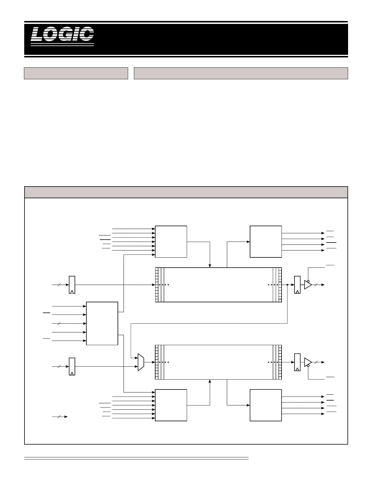
LF3304 BLOCK DIAGRAM
DESCRIPTION
The LF3304 is a dual line buffer/
FIFO, designed to operate at HDTV
rates. The LF3304 will operate in
two distinct modes: Line Buffer and
FIFO. In these modes the two memo-
ries can operate independently or
with common control.
The LF3304 comprises two 12-bit 4K
memories configurable in a variety of
ways including: Two 12-bit 4K deep
line buffers (independent lengths),
Three 8-bit 4K deep line buffers
(common lengths), One 12-bit 8K
deep line buffer, or Two 12-bit 4K
FIFOs (independent operation).
In FIFO mode, independent Read
and Write Resets give the designer
control over the internal pointers
providing flexibility not commonly
found in ordinary FIFOs.
The LF3304 operatates at a maximum
data rate of 100 MHz and is available
in a 100-lead PQFP package.
12
AIN11-0
ADDRA
LDA
LENGTH11-0
ADDRB
LDB
12
12
BIN11-0
MODE1-0
2
WCLKA
RCLKA
WENA
RENA
RRA
RWA
MASTER
CONTROL
WCLKB
RCLKB
WENB
RENB
RRB
RWB
RAM ARRAY 1
CONTROL
FLAG
GENERATOR
VARIABLE LENGTH RAM ARRAY A
4K x 12-bit
FFA
EFA
PAFA
PAEA
OEA
12
AOUT11-0
VARIABLE LENGTH RAM ARRAY B
4K x 12-bit
RAM ARRAY 2
CONTROL
FLAG
GENERATOR
12
BOUT11-0
OEB
FFB
EFB
PAFB
PAEB
Video Imaging Products
1 08/16/2000–LDS.3304-F
1 page 
DEVICES INCORPORATED
LF3304
Dual Line Buffer/FIFO
FIFO MODE
OPERATION
Initialization
Upon power-up, the LF3304 requires
the initialization of the internal read
and write address pointers. This
initialization sequence can be done
by either a Flag Enable Reset or a
Flag Disable Reset.
A Flag Enable Reset will force the
FIFO to operate in a ‘Flag Enabled’
mode. In this mode, writing will be
disabled when FFx is LOW and
reading is disabled when EFx is
LOW. Any ‘write beyond full’ event
or ‘read beyond empty’ event will be
disabled. Note: in an ‘empty’ state,
the last data word read from the
FIFO is held on the output bus until
the next valid read cycle.
A Flag Disable Reset will force the
FIFO to operate in a ‘Flag Disabled’
mode. In this mode, the user is
allowed to write over previously un-
read data and read out previously
read data. Consequently, any
enabled write or read is valid thus
allowing the write and read pointers
to ‘wrap-around’. Note: due to the
nature of this mode, the flag status
should be disregarded. For example,
as the 4096th data word is written
into the FIFO, assuming that no
preceding read cycles have occured,
FFx will be driven LOW thus indicat-
ing a ‘full’state. While the FIFO is
still in this ‘full’ state, the next
enabled write will access address
000H, thus writing over data that
has not yet been read out.
Flag Enable Reset
A Flag Enable Reset resets the read
and write pointers and enables the
flags to control the reading and
writing of data according to the Full
Flag and Empty Flag conditions. A
Flag Enable Reset occurs when the
following conditions are met:
1. RWA/RWB must be LOW for at
least one WCLKA/WCLKB cycle.
2. RRA/RRB must be LOW for at
least one RCLKA/RCLKB cycle.
3. WENx and RENx must be HIGH
during the above two conditions
plus one addition write or read
cycle (which ever is longer).
The Flag Enable Reset condition can
be disabled if one of the two Flag
Disable Reset conditions are applied.
Flag Disable Reset
A Flag Disable Reset resets the read
and write pointers and disables the
flags from controlling the reading
and writing of data. A Flag Disable
Reset occurs when the following
conditions are met:
1. RWA/RWB must be LOW for at
least one WCLKA/WCLKB cycle
while WENx is LOW.
2. RRA/RRB must be LOW for at
least one RCLKA/RCLKB cycle
while RENx is LOW.
Configuration of Programmable Flags
In order to load a FIFO A Program-
mable Flag Register, a rising edge of
WCLKA, while WENA is LOW,
latches AIN11-0 into either the PAFA
or PAEA Register - depending on the
states of ADDRA and LDA (See
Table 2).
In order to load a FIFO B Program-
mable Flag Register, a rising edge of
WCLKB, while WENB is LOW,
latches BIN11-0 into either the PAFB
or PAEB Register - depending on the
states of ADDRB and LDB (See Table
2). See the Figure labeled “Program-
mable Flag Load Timing.”
Video Imaging Products
5 08/16/2000–LDS.3304-F
5 Page 
DEVICES INCORPORATED
LF3304
Dual Line Buffer/FIFO
NOTES
1. Maximum Ratings indicate stress
specifications only. Functional oper-
ation of these products at values beyond
those indicated in the Operating Condi-
tions table is not implied. Exposure to
maximum rating conditions for ex-
tended periods may affect reliability.
2. The products described by this spec-
ification include internal circuitry de-
signedtoprotect the chipfromdamaging
substrate injection currents and accu-
mulations of static charge. Neverthe-
less, conventional precautions should
be observed during storage, handling,
and use of these circuits in order to avoid
exposure to excessive electrical stress
values.
3. This device provides hard clamping
of transient undershoot. Input levels
below ground will be clamped begin-
ning at –0.6 V. The device can withstand
indefinite operation with inputs or out-
puts in the range of –0.5 V to +5.5 V.
Device operation will not be adversely
affected, however, input current levels
will be well in excess of 100 mA.
input transition times less than 3 ns,
output reference levels of 1.5 V (except
tDIS test), and input levels of nominally
0 to 3.0 V. Output loading may be a
resistive divider which provides for
specified IOH and IOL at an output
voltage of VOH min and VOL max
respectively. Alternatively, a diode
bridge with upper and lower current
sources of IOH and IOL respectively,
and a balancing voltage of 1.5 V may be
used. Parasitic capacitance is 30 pF
minimum, and may be distributed.
This device has high-speed outputs ca-
pable of large instantaneous current
pulses and fast turn-on/turn-off times.
As a result, care must be exercised in the
testing of this device. The following
measures arerecommended:
a. A 0.1 µF ceramic capacitor should be
installed between VCC and Ground
leads as close to the Device Under Test
(DUT) as possible. Similar capacitors
should be installed between device VCC
and the tester common, and device
ground and tester common.
measured to the 1.5 V crossing point with
datasheet loads. For the tDIS test, the
transition is measured to the ±200mV
level from the measured steady-state
output voltage with ±10mA loads.
The balancing voltage, VTH, is set at
3.0 V for Z-to-0 and 0-to-Z tests, and
set at 0 V for Z-to-1 and 1-to-Z tests.
12. These parameters are only tested at
the high temperature extreme, which is
the worst case for leakage current.
FIGURE A. OUTPUT LOADING CIRCUIT
S1
DUT
CL
IOL
VTH
IOH
FIGURE B. THRESHOLD LEVELS
tENA
tDIS
OE 1.5 V
1.5 V
4. Actual test conditions may vary from b. Ground and VCC supply planes must
those designated but operation is guar- be brought directly to the DUT socket or
anteed as specified.
contactor fingers.
5. Supply current for a given applica-
tion can be accurately approximated
by:
NCV2 F
where
4
N = total number of device outputs
C = capacitive load per output
V = supply voltage
F = clock frequency
6. Tested with outputs changing every
cycle and no load, at a 40 MHz clock rate.
7. Tested with all inputs within 0.1 V of
VCC or Ground, no load.
8. These parameters are guaranteed but
not 100% tested.
9. AC specifications are tested with
c. Input voltages on a test fixture should
be adjusted to compensate for inductive
ground and VCC noise to maintain re-
quired DUT input levels relative to the
DUT ground pin.
10. Each parameter is shown as a mini-
mum or maximum value. Input require-
ments are specified from the point of view
of the external system driving the chip.
Setup time, for example, is specified as a
minimum since the external system must
supply at least that much time to meet the
worst-case requirements of all parts.
Responses from the internal circuitry are
specified from the point of view of the
device. Output delay, for example, is
specified as a maximum since worst-
case operation of any device always pro-
vides data within that time.
11. For the tENA test, the transition is
Z0
1.5 V
VOL* 0.2 V
3.0V Vth
0Z
Z1
1.5 V
VOH* 0.2 V
1Z
0V Vth
VOL* Measured VOL with IOH = –10mA and IOL = 10mA
VOH* Measured VOH with IOH = –10mA and IOL = 10mA
Video Imaging Products
11 08/16/2000–LDS.3304-F
11 Page | ||
| Páginas | Total 12 Páginas | |
| PDF Descargar | [ Datasheet LF3304.PDF ] | |
Hoja de datos destacado
| Número de pieza | Descripción | Fabricantes |
| LF3304 | Dual Line Buffer/FIFO | LOGIC Devices Incorporated |
| Número de pieza | Descripción | Fabricantes |
| SLA6805M | High Voltage 3 phase Motor Driver IC. |
Sanken |
| SDC1742 | 12- and 14-Bit Hybrid Synchro / Resolver-to-Digital Converters. |
Analog Devices |
|
DataSheet.es es una pagina web que funciona como un repositorio de manuales o hoja de datos de muchos de los productos más populares, |
| DataSheet.es | 2020 | Privacy Policy | Contacto | Buscar |