|
|
|
PDF NCP5393A Data sheet ( Hoja de datos )
| Número de pieza | NCP5393A | |
| Descripción | 2/3/4-Phase Controller | |
| Fabricantes | ON Semiconductor | |
| Logotipo | ||
Hay una vista previa y un enlace de descarga de NCP5393A (archivo pdf) en la parte inferior de esta página. Total 24 Páginas | ||
|
No Preview Available !
NCP5393Awww.DataSheet4U.com
Product Preview
2/3/4-Phase Controller for
CPU Applications
The NCP5393A is a multiphase synchronous buck regulator
controller designed to power the Core and Northbridge of an AMD
microprocessor. The controller has a user configurable two, three, or
four phase regulator for the Core and an independent single phase
regulator to power the microprocessor Northbridge. The NCP5393A
incorporates differential voltage sensing, differential phase current
sensing, optional load−line voltage positioning, and programmable
VDD and VDDNB offsets to provide accurately regulated power
parallel− and serial−VID AMD processors. Dual−edge multiphase
modulation provides the fastest initial response to dynamic load
events. This reduces system cost by requiring less bulk and ceramic
output capacitance to meet transient regulation specifications.
High performance operational error amplifiers are provided to
simplify compensation of the VDD and VDDNB regulators. Dynamic
Reference Injection further simplifies loop compensation by
eliminating the need to compromise between response to load
transients and response to VID code changes.
Features
• Meets AMD’s Hybrid VR Specifications
• Up to Four VDD Phases
• Single−Phase VDDNB Controller
• Dual−Edge PWM for Fastest Initial Response to Transient Loading
• High Performance Operational Error Amplifiers
• Internal Soft Start and Slew Rate Limiting
• Dynamic Reference Injection (Patent #US07057381)
• DAC Range from 12.5 mV to 1.55 V
• $0.5% DAC Accuracy fro 0.8 V to 1.55 V
• VDD and VDD Offset Ranges 0 mV − 800 mV
• True Differential Remote Voltage Sense Amplifiers
• Phase−to−Phase IDD Current Balancing
• Differential Current Sense Amplifiers for Each Phase of Each Output
• “Lossless” Inductor Current Sensing for VDD and VDDNB Outputs
• Supports Load Lines (Droop) for VDD and VDDNB Outputs
• Oscillator Range of 100 kHz − 1 MHz
• Tracking Over Voltage Protection
• Output Inductor DCR−Based Over Current Protection for VDD and
VDDNB Outputs
• Guaranteed Startup into Precharged Loads
• Temperature Range: 0°C to 70°C
• This is a Pb−Free Device
Applications
• Desktop Processors
• Server Processors
• High−End Notebook PCs
This document contains information on a product under development. ON Semiconductor
reserves the right to change or discontinue this product without notice.
http://onsemi.com
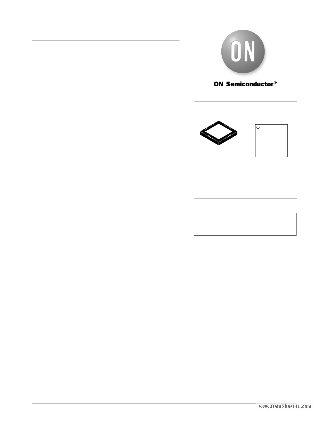
MARKING
DIAGRAM
1
1 48
QFN48, 7x7
CASE 485AJ
NCP5393A
AWLYYWWG
A = Assembly Location
WL = Wafer Lot
YY = Year
WW = Work Week
G = Pb−Free Package
ORDERING INFORMATION
Device
Package
Shipping†
NCP5393AMNR2G QFN48 2500 / Tape & Reel
(Pb−Free)
†For information on tape and reel specifications,
including part orientation and tape sizes, please
refer to our Tape and Reel Packaging Specifications
Brochure, BRD8011/D.
© Semiconductor Components Industries, LLC, 2008
August, 2008 − Rev. P0
1
Publication Order Number:
NCP5393A/D
1 page 
NCP5393A
www.DataSNhCePet543U9.c3oAmPIN DESCRIPTIONS
Pin No.
Symbol
Description
1
VCCA
5 V supply pin for the NCP5393A. The VCC bypassing capacitance must be connected between this
pin and GND (preferably returned to the package flag).
2
GND
Small−signal power supply return. This pin should be tied directly to the package flag (exposed pad).
3
COMP
Output of the voltage error amplifier for the VDD regulator.
4 FB Voltage error amplifier inverting input for the VDD regulator.
5
DROOP
Voltage output signal proportional to total current drawn from the VDD regulator. Used when load line
operation (“droop”) is desired.
6 VS+ Non−inverting input to the differential remote sense amplifier for the VDD regulator.
7 VS− Inverting input to the differential remote sense amplifier for the VDD regulator.
8
OFFSET
Input for offset voltage to be added to the VDD DAC’s output voltage. Ground this pin for zero VDD
offset.
9
DIFFOUT
Output of the differential remote sense amplifier for the VDD regulator.
10
VFIX
When pulled low, this pin causes the levels on the SVC (VID3) and SVD (VID2) pins to be decoded
as a two−bit DAC code, which controls the VDD and VDDNB outputs. Internally pulled high by 5 mA to
VCC
11
12VMON
UVLO monitor input for the 12 V power rail.
12
PSI_L
Determines number of phases operating in PSI_L mode. Phase shed count is locked upon ENABLE
assertion. After soft−start, becomes power saving control in PVID mode. Low = phase shed
operation, High = normal operation.
13 CS1 Non−inverting input to current sense amplifier #1 for the VDD regulator. See Table: “Pin Connections
vs. Phase Count”
14
CS1N
Inverting input to current sense amplifier #1 for the VDD regulator. See Table: “Pin Connections vs.
Phase Count”
15 CS2 Non−inverting input to current sense amplifier #2 for the VDD regulator. See Table: “Pin Connections
vs. Phase Count”
16
CS2N
Inverting input to current sense amplifier #2 for the VDD regulator. See Table: “Pin Connections vs.
Phase Count”
17 CS3 Non−inverting input to current sense amplifier #3 for the VDD regulator. See Table: “Pin Connections
vs. Phase Count”
18
CS3N
Inverting input to current sense amplifier #3 for the VDD regulator. See Table: “Pin Connections vs.
Phase Count”
19 CS4 Non−inverting input to current sense amplifier #4 for the VDD regulator. See Table: “Pin Connections
vs. Phase Count”
20
CS4N
Inverting input to current sense amplifier #4 for the VDD regulator. See Table: “Pin Connections vs.
Phase Count”
21
ILIM
Overcurrent shutdown threshold for VDD and VDDNB. A resistor divider from ROSC to GND is
typically used to develop an appropriate voltage on ILIM.
22
VCCB
5 V supply pin. Tie this pin to VCCA (Pin 1).
23
NB_CS
Non−inverting input to the current sense amplifier for the VDDNB regulator
24
NB_CSN
Inverting input to the current sense amplifier for the VDDNB regulator
25
VID4
Parallel Voltage ID DAC Input 4. Not used in SVI mode.
26
VID5
Parallel Voltage ID DAC Input 5. Not used in SVI mode.
27
ROSC
A resistance from this pin to ground programs the VDD and VDDNB oscillator frequencies. This pin
supplies a trimmed output voltage of 2 V.
28 NB_DIFFOUT Output of the differential remote sense amplifier for the VDDNB regulator.
29
NB_OFFSET
Input for offset voltage to be added to the VDDNB DAC’s output voltage. Ground this pin for zero
VDDNB offset.
30
NB_VS−
Inverting input to the differential remote sense amplifier for the VDDNB regulator.
31
NB_VS+
Non−inverting input to the differential remote sense amplifier for the VDDNB regulator.
http://onsemi.com
5
5 Page 
NCP5393A
www.DataSEhLeEeCt4TUR.cIoCmAL CHARACTERISTICS (Unless otherwise stated: 0°CvTAv70°C; 4.75 VvVCCv5.25 V; All DAC Codes; CVCC = 0.1 mF)
Parameter
Test Conditions
Min Typ Max Unit
PSI_L (Power Saving Phase Shed and Control, Active Low) (This pin is used in PVI mode only)
PSI_L Hysteresis
CURRENT LIMIT
After Soft−Start, VHIGH − VLOW or VLOW − VHIGH
100 mV
Current Sense Amp to ILIM Gain
ILIM Pin Input Bias Current
20 mV < (CSx − CSxN) < 60 mV (CS inputs tied)
5.7 6.0 6.3 V/V
− − 0.5 mA
ILIM Pin Working Voltage Range
(Note 3)
0.2 − 2.0 V
ILIM Offset Voltage
Offset extrapolated to CSx−CSxN = 0 V, and referred
−
30
− mV
to the ILIM pin
Delay
− 600 −
ns
VDDNB Current Limit Coefficient
OFFSET INPUTS (VDD & VDDNB)
Output Offset Voltage Above VDAC
= N x VNBILIM /VILIM, where N = number of VDD
phases, and VNBILIM is the equivalent voltage
threshold for NB Current Limit resulting from VILIM.
1.0 V
0 − 800 mV
OUTPUT OVERVOLTAGE PROTECTION (VDD & VDDNB)
Over Voltage Threshold
In normal operation, with no VID changes
VDAC
+ 220
VDAC
+ 235
VDAC
+ 250
mV
VCCA UNDERVOLTAGE PROTECTION
VCCA UVLO Start Threshold
4.0 4.25 4.5
V
VCCA UVLO Stop Threshold
3.8 4.05 4.3
V
VCCA UVLO Hysteresis
200 mV
INPUT SUPPLY CURRENT
VCC Operating Current
ENABLE held Low, No PWM operation
− 25 35 mA
12VMON
12VMON (High Threshold)
8 8.5 9
V
12VMON (Low Threshold)
7 7.5 8
V
12VMON Hysteresis
Low − High or High − Low
1.0 V
3. Guaranteed by design. Not production tested.
TYPICAL CHARACTERISTICS
2.03 1.5
1.4
2.01
1.3 Enable Increasing Voltage
1.99
1.2
1.97 1.1 Enable Decreasing Voltage
1.95
0
1.0
25 50 75 0
25 50 75
TJ, JUNCTION TEMPERATURE (°C)
Figure 1. SS Time vs. Temperature
TJ, JUNCTION TEMPERATURE (°C)
Figure 2. Enable Threshold Voltage vs.
Temperature
http://onsemi.com
11
11 Page | ||
| Páginas | Total 24 Páginas | |
| PDF Descargar | [ Datasheet NCP5393A.PDF ] | |
Hoja de datos destacado
| Número de pieza | Descripción | Fabricantes |
| NCP5393 | 2/3/4-Phase Controller | ON Semiconductor |
| NCP5393A | 2/3/4-Phase Controller | ON Semiconductor |
| NCP5393B | 2/3/4-Phase Controller | ON Semiconductor |
| Número de pieza | Descripción | Fabricantes |
| SLA6805M | High Voltage 3 phase Motor Driver IC. |
Sanken |
| SDC1742 | 12- and 14-Bit Hybrid Synchro / Resolver-to-Digital Converters. |
Analog Devices |
|
DataSheet.es es una pagina web que funciona como un repositorio de manuales o hoja de datos de muchos de los productos más populares, |
| DataSheet.es | 2020 | Privacy Policy | Contacto | Buscar |