|
|
PDF MAX11609 Data sheet ( Hoja de datos )
| Número de pieza | MAX11609 | |
| Descripción | (MAX11606 - MAX11611) 4-/8-/12-Channel ADCs | |
| Fabricantes | Maxim Integrated Products | |
| Logotipo |  |
|
Hay una vista previa y un enlace de descarga de MAX11609 (archivo pdf) en la parte inferior de esta página. Total 21 Páginas | ||
|
No Preview Available !
19-4560; Rev 0; 4/09
www.DataSheet4U.com
2.7V to 3.6V and 4.5V to 5.5V, Low-Power,
4-/8-/12-Channel, 2-Wire Serial 10-Bit ADCs
General Description
The MAX11606–MAX11611 low-power, 10-bit, multichan-
nel analog-to-digital converters (ADCs) feature internal
track/hold (T/H), voltage reference, clock, and an
I2C-compatible 2-wire serial interface. These devices
operate from a single supply of 2.7V to 3.6V (MAX11607/
MAX11609/MAX11611) or 4.5V to 5.5V (MAX11606/
MAX11608/MAX11610) and require only 670µA at the
maximum sampling rate of 94.4ksps. Supply current falls
below 230µA for sampling rates under 46ksps.
AutoShutdown™ powers down the devices between conver-
sions, reducing supply current to less than 1µA at low
throughput rates. The MAX11606/MAX11607 have 4 analog
input channels each, the MAX11608/MAX11609 have 8 ana-
log input channels each, while the MAX11610/MAX11611
have 12 analog input channels each. The fully differential
analog inputs are software configurable for unipolar or bipo-
lar, and single ended or differential operation.
The full-scale analog input range is determined by the
internal reference or by an externally applied reference
voltage ranging from 1V to VDD. The MAX11607/
MAX11609/MAX11611 feature a 2.048V internal reference
and the MAX11606/MAX11608/MAX11610 feature a
4.096V internal reference.
The MAX11606/MAX11607 are available in an 8-pin
µMAX® package. The MAX11608–MAX11611 are avail-
able in a 16-pin QSOP package. The MAX11606–
MAX11611 are guaranteed over the extended tempera-
ture range (-40°C to +85°C). For pin-compatible 12-bit
parts, refer to the MAX11612–MAX11617 data sheet. For
pin-compatible 8-bit parts, refer to the MAX11600–
MAX11605 data sheet.
Handheld Portable
Applications
Medical Instruments
Battery-Powered Test
Equipment
Applications
Solar-Powered Remote
Systems
Received-Signal-Strength
Indicators
System Supervision
Features
o High-Speed I2C-Compatible Serial Interface
400kHz Fast Mode
1.7MHz High-Speed Mode
o Single-Supply
2.7V to 3.6V (MAX11607/MAX11609/MAX11611)
4.5V to 5.5V (MAX11606/MAX11608/MAX11610)
o Internal Reference
2.048V (MAX11607/MAX11609/MAX11611)
4.096V (MAX11606/MAX11608/MAX11610)
o External Reference: 1V to VDD
o Internal Clock
o 4-Channel Single-Ended or 2-Channel Fully
Differential (MAX11606/MAX11607)
o 8-Channel Single-Ended or 4-Channel Fully
Differential (MAX11608/MAX11609)
o 12-Channel Single-Ended or 6-Channel Fully
Differential (MAX11610/MAX11611)
o Internal FIFO with Channel-Scan Mode
o Low Power
670µA at 94.4ksps
230µA at 40ksps
60µA at 10ksps
6µA at 1ksps
0.5µA in Power-Down Mode
o Software-Configurable Unipolar/Bipolar
o Small Packages
8-Pin µMAX (MAX11606/MAX11607)
16-Pin QSOP (MAX11608–MAX11611)
Ordering Information
PART
TEMP RANGE PIN-
I2C SLAVE
PACKAGE ADDRESS
MAX11606EUA+ -40°C to +85°C 8 µMAX
MAX11607EUA+ -40°C to +85°C 8 µMAX
0110100
0110100
MAX11608EEE+* -40°C to +85°C 16 QSOP 0110011
MAX11609EEE+* -40°C to +85°C 16 QSOP
MAX11610EEE+* -40°C to +85°C 16 QSOP
0110011
0110101
MAX11611EEE+* -40°C to +85°C 16 QSOP 0110101
+Denotes a lead(Pb)-free/RoHs-compliant package.
*Future product—contact factory for availability.
AutoShutdown is a trademark of Maxim Integrated Products, Inc.
µMAX is a registered trademark of Maxim Integrated Products, Inc.
Pin Configurations, Typical Operating Circuit, and Selector
Guide appear at end of data sheet.
________________________________________________________________ Maxim Integrated Products 1
For pricing, delivery, and ordering information, please contact Maxim Direct at 1-888-629-4642,
or visit Maxim’s website at www.maxim-ic.com.
1 page 
www.DataSheet4U.com
2.7V to 3.6V and 4.5V to 5.5V, Low-Power,
4-/8-/12-Channel, 2-Wire Serial 10-Bit ADCs
TIMING CHARACTERISTICS (Figure 1) (continued)
(VDD = 2.7V to 3.6V (MAX11607/MAX11609/MAX11611), VDD = 4.5V to 5.5V (MAX11606/MAX11608/MAX11610), VREF = 2.048V
(MAX11607/MAX11609/MAX11611), VREF = 4.096V (MAX11606/MAX11608/MAX11610), fSCL = 1.7MHz, TA = TMIN to TMAX, unless other-
wise noted. Typical values are at TA = +25°C. See Tables 1–5 for programming notation.)
PARAMETER
SYMBOL
CONDITIONS
MIN TYP MAX UNITS
Rise Time of SCL Signal
(Current Source Enabled)
tRCL Measured from 0.3VDD to 0.7VDD
20 80 ns
Rise Time of SCL Signal after
Acknowledge Bit
tRCL1 Measured from 0.3VDD to 0.7VDD
20 160 ns
Fall Time of SCL Signal
Rise Time of SDA Signal
Fall Time of SDA Signal
Setup Time for STOP (P) Condition
Capacitive Load for Each Bus Line
Pulse Width of Spike Suppressed
tFCL
tRDA
tFDA
tSU,STO
CB
tSP
Measured from 0.3VDD to 0.7VDD
Measured from 0.3VDD to 0.7VDD
Measured from 0.3VDD to 0.7VDD (Note 11)
(Notes 10 and 13)
20
20
20
160
0
80 ns
160 ns
160 ns
ns
400 pF
10 ns
Note 1:
Note 2:
Note 3:
Note 4:
Note 5:
Note 6:
Note 7:
Note 8:
For DC accuracy, the MAX11606/MAX11608/MAX11610 are tested at VDD = 5V and the MAX11607/MAX11609/MAX11611
are tested at VDD = 3V. All devices are configured for unipolar, single-ended inputs.
Relative accuracy is the deviation of the analog value at any code from its theoretical value after the full-scale range and
offsets have been calibrated.
Offset nulled.
Conversion time is defined as the number of clock cycles needed for conversion multiplied by the clock period. Conversion
time does not include acquisition time. SCL is the conversion clock in the external clock mode.
A filter on the SDA and SCL inputs suppresses noise spikes and delays the sampling instant.
The absolute input-voltage range for the analog inputs (AIN0–AIN11) is from GND to VDD.
When the internal reference is configured to be available at AIN_/REF (SEL[2:1] = 11), decouple AIN_/REF to GND with a
0.1µF capacitor and a 2kΩ series resistor (see the Typical Operating Circuit).
ADC performance is limited by the converter’s noise floor, typically 300µVP-P.
Note 9: Measured as follows for the MAX11607/MAX11609/MAX11611:
[ ]⎡
⎢
⎣
VFS(3.6V) − VFS(2.7V)
×
2N −1⎤
VREF
⎥
⎦
(3.6V − 2.7V)
and for the MAX11606/MAX11608/MAX11610, where N is the number of bits:
[ ]⎡
⎢
⎣
VFS(5.5V) − VFS(4.5V)
×
2N −1⎤
VREF
⎥
⎦
(5.5V − 4.5V)
Note 10: A master device must provide a data hold time for SDA (referred to VIL of SCL) to bridge the undefined region of SCL’s
falling edge (see Figure 1).
Note 11: The minimum value is specified at TA = +25°C.
Note 12: CB = total capacitance of one bus line in pF.
Note 13: fSCL must meet the minimum clock low time plus the rise/fall times.
_______________________________________________________________________________________ 5
5 Page 
www.DataSheet4U.com
2.7V to 3.6V and 4.5V to 5.5V, Low-Power,
4-/8-/12-Channel, 2-Wire Serial 10-Bit ADCs
swing from (GND - 0.3V) to (VDD + 0.3V) without caus-
ing damage to the device. For accurate conversions
the inputs must not go more than 50mV below GND or
above VDD.
Single-Ended/Differential Input
The SGL/DIF of the configuration byte configures the
MAX11606–MAX11611 analog-input circuitry for single-
ended or differential inputs (Table 2). In single-ended
mode (SGL/DIF = 1), the digital conversion results are
the difference between the analog input selected by
CS[3:0] and GND (Table 3). In differential mode (SGL/
DIF = 0), the digital conversion results are the differ-
ence between the + and the - analog inputs selected
by CS[3:0] (Table 4).
Unipolar/Bipolar
When operating in differential mode, the BIP/UNI bit of
the setup byte (Table 1) selects unipolar or bipolar
operation. Unipolar mode sets the differential input
range from 0 to VREF. A negative differential analog
input in unipolar mode causes the digital output code
to be zero. Selecting bipolar mode sets the differential
input range to ±VREF/2. The digital output code is bina-
ry in unipolar mode and two’s complement in bipolar
mode. See the Transfer Functions section.
In single-ended mode, the MAX11606–MAX11611
always operate in unipolar mode irrespective of
BIP/UNI. The analog inputs are internally referenced to
GND with a full-scale input range from 0 to VREF.
2-Wire Digital Interface
The MAX11606–MAX11611 feature a 2-wire interface
consisting of a serial-data line (SDA) and serial-clock line
(SCL). SDA and SCL facilitate bidirectional communica-
tion between the MAX11606–MAX11611 and the master
at rates up to 1.7MHz. The MAX11606–MAX11611 are
slaves that transfer and receive data. The master (typi-
cally a microcontroller) initiates data transfer on the bus
and generates the SCL signal to permit that transfer.
SDA and SCL must be pulled high. This is typically done
with pullup resistors (750Ω or greater) (see the Typical
Operating Circuit). Series resistors (RS) are optional.
They protect the input architecture of the MAX11606–
MAX11611 from high voltage spikes on the bus lines,
minimize crosstalk, and undershoot of the bus signals.
Bit Transfer
One data bit is transferred during each SCL clock
cycle. A minimum of 18 clock cycles are required to
transfer the data in or out of the MAX11606–
MAX11611. The data on SDA must remain stable dur-
ing the high period of the SCL clock pulse. Changes in
SDA while SCL is stable are considered control signals
(see the START and STOP Conditions section). Both
SDA and SCL remain high when the bus is not busy.
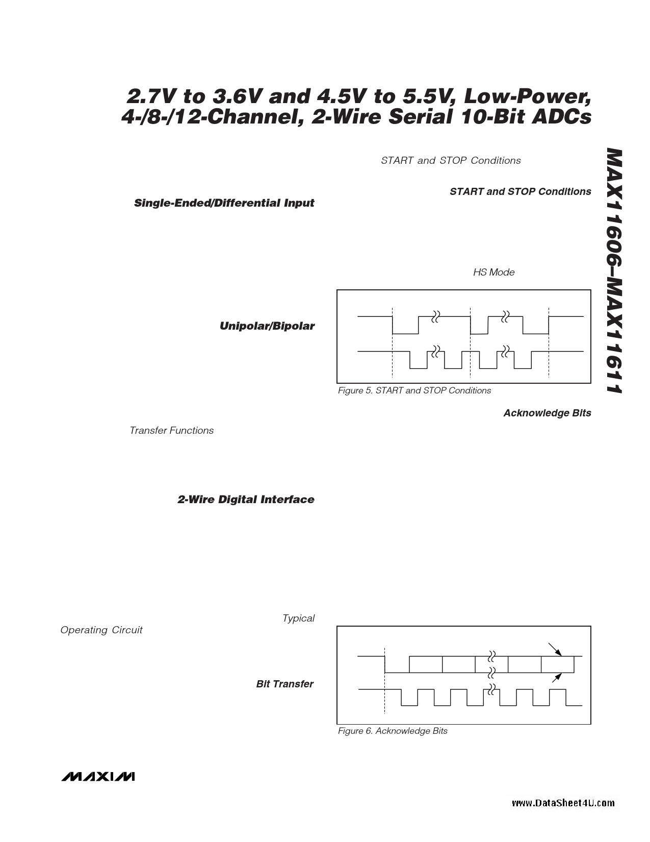
START and STOP Conditions
The master initiates a transmission with a START condi-
tion (S), a high-to-low transition on SDA while SCL is high.
The master terminates a transmission with a STOP condi-
tion (P), a low-to-high transition on SDA while SCL is high
(Figure 5). A repeated START condition (Sr) can be used
in place of a STOP condition to leave the bus active and
the mode unchanged (see the HS Mode section).
S Sr
P
SDA
SCL
Figure 5. START and STOP Conditions
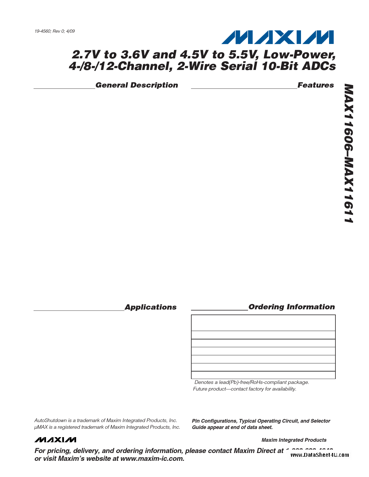
Acknowledge Bits
Data transfers are acknowledged with an acknowledge
bit (A) or a not-acknowledge bit (A). Both the master
and the MAX11606–MAX11611 (slave) generate
acknowledge bits. To generate an acknowledge, the
receiving device must pull SDA low before the rising
edge of the acknowledge-related clock pulse (ninth
pulse) and keep it low during the high period of the
clock pulse (Figure 6). To generate a not-acknowledge,
the receiver allows SDA to be pulled high before the
rising edge of the acknowledge-related clock pulse
and leaves SDA high during the high period of the
clock pulse. Monitoring the acknowledge bits allows for
detection of unsuccessful data transfers. An unsuc-
cessful data transfer happens if a receiving device is
busy or if a system fault has occurred. In the event of
an unsuccessful data transfer, the bus master should
reattempt communication at a later time.
S
SDA
SCL
12
NOT ACKNOWLEDGE
ACKNOWLEDGE
89
Figure 6. Acknowledge Bits
______________________________________________________________________________________ 11
11 Page | ||
| Páginas | Total 21 Páginas | |
| PDF Descargar | [ Datasheet MAX11609.PDF ] | |
Hoja de datos destacado
| Número de pieza | Descripción | Fabricantes |
| MAX1160 | 10-Bit / 20Msps / TTL-Output ADC | Maxim Integrated |
| MAX11600 | (MAX11600 - MAX11605) 2-Wire Serial 8-Bit ADCs | Maxim Integrated Products |
| MAX11601 | (MAX11600 - MAX11605) 2-Wire Serial 8-Bit ADCs | Maxim Integrated Products |
| MAX11602 | (MAX11600 - MAX11605) 2-Wire Serial 8-Bit ADCs | Maxim Integrated Products |
| Número de pieza | Descripción | Fabricantes |
| SLA6805M | High Voltage 3 phase Motor Driver IC. |
Sanken |
| SDC1742 | 12- and 14-Bit Hybrid Synchro / Resolver-to-Digital Converters. |
Analog Devices |
|
DataSheet.es es una pagina web que funciona como un repositorio de manuales o hoja de datos de muchos de los productos más populares, |
| DataSheet.es | 2020 | Privacy Policy | Contacto | Buscar |
