|
|
PDF A25L016 Data sheet ( Hoja de datos )
| Número de pieza | A25L016 | |
| Descripción | 16Mbit Low Voltage | |
| Fabricantes | AMIC Technology | |
| Logotipo |  |
|
Hay una vista previa y un enlace de descarga de A25L016 (archivo pdf) en la parte inferior de esta página. Total 30 Páginas | ||
|
No Preview Available !
www.DataSheet4U.com
A25L016 Series
16Mbit Low Voltage, Serial Flash Memory
With 100MHz Uniform 4KB Sectors
Document Title
16Mbit, Low Voltage, Serial Flash Memory With 100MHz Uniform 4KB Sectors
Revision History
Rev. No. History
0.0 Initial issue
Issue Date
April 2, 2008
Remark
Final
(April, 2008, Version 0.0)
AMIC Technology Corp.
1 page 
www.DataSheet4U.com
SPI MODES
These devices can be driven by a microcontroller with its SPI
peripheral running in either of the two following modes:
– CPOL=0, CPHA=0
– CPOL=1, CPHA=1
For these two modes, input data is latched in on the rising
edge of Serial Clock (C), and output data is available from the
A25L016 Series
falling edge of Serial Clock (C).
The difference between the two modes, as shown in Figure 2,
is the clock polarity when the bus master is in Stand-by mode
and not transferring data:
– C remains at 0 for (CPOL=0, CPHA=0)
– C remains at 1 for (CPOL=1, CPHA=1)
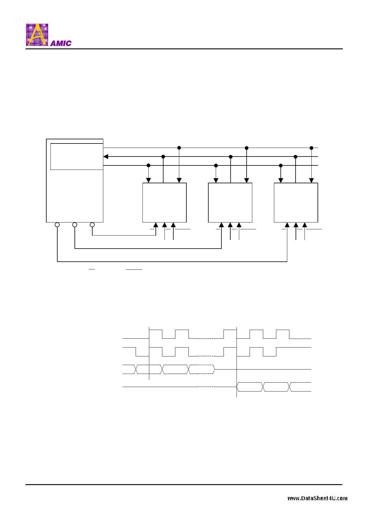
Figure 1. Bus Master and Memory Devices on the SPI Bus
SPI Interface with
(CPOL, CPHA)
= (0, 0) or (1, 1)
SDO
SDI
SCK
Bus Master
(ST6, ST7, ST9,
ST10, Other)
CS3 CS2 CS1
C DO DIO
SPI Memory
Device
S W HOLD
C DO DIO
SPI Memory
Device
S W HOLD
C DO DIO
SPI Memory
Device
S W HOLD
Note: The Write Protect ( W ) and Hold ( HOLD ) signals should be driven, High or Low as appropriate.
Figure 2. SPI Modes Supported
CPOL CPHA
00
C
11
C
DIO
DO
MSB
MSB
(April, 2008, Version 0.0)
4 AMIC Technology Corp.
5 Page 
www.DataSheet4U.com
A25L016 Series
INSTRUCTIONS
All instructions, addresses and data are shifted in and out of
the device, most significant bit first.
Serial Data Input (DIO) is sampled on the first rising edge of
Serial Clock (C) after Chip Select ( S ) is driven Low. Then, the
one-byte instruction code must be shifted in to the device,
most significant bit first, on Serial Data Input (DIO), each bit
being latched on the rising edges of Serial Clock (C).
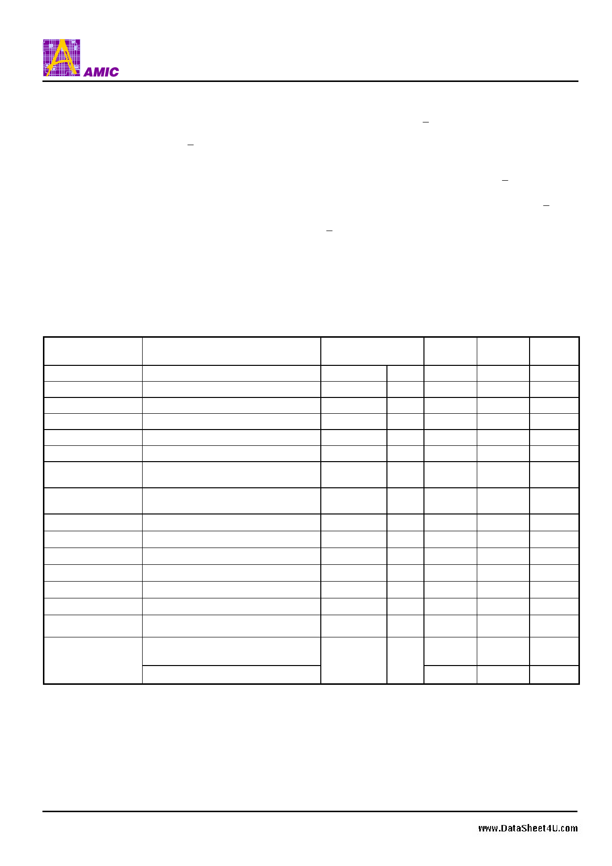
The instruction set is listed in Table 3.
Every instruction sequence starts with a one-byte instruction
code. Depending on the instruction, this might be followed by
address bytes, or by data bytes, or by both or none.
In the case of a Read Data Bytes (READ), Read Data Bytes at
Higher Speed (Fast_Read), Read Identification (RDID), Read
Electronic Manufacturer and Device Identification (REMS),
Read Status Register (RDSR) or Release from Deep
Power-down, Read Device Identification and Read Electronic
Signature (RES) instruction,
the shifted-in instruction sequence is followed by a data-out
sequence. Chip Select ( S ) can be driven High after any bit of
the data-out sequence is being shifted out.
In the case of a Page Program (PP), Sector Erase (SE), Block
Erase (BE), Chip Erase (CE), Write Status Register (WRSR),
Write Enable (WREN), Write Disable (WRDI) or Deep
Power-down (DP) instruction, Chip Select ( S ) must be driven
High exactly at a byte boundary, otherwise the instruction is
rejected, and is not executed. That is, Chip Select ( S ) must
driven High when the number of clock pulses after Chip Select
( S ) being driven Low is an exact multiple of eight.
All attempts to access the memory array during a Write Status
Register cycle, Program cycle or Erase cycle are ignored, and
the internal Write Status Register cycle, Program cycle or
Erase cycle continues unaffected.
Table 3. Instruction Set
Instruction
Description
One-byte
Instruction Code
Address
Bytes
WREN
Write Enable
0000 0110 06h
0
WRDI
Write Disable
0000 0100 04h
0
RDSR
Read Status Register
0000 0101 05h
0
WRSR
Write Status Register
0000 0001 01h
0
READ
Read Data Bytes
0000 0011 03h
3
FAST_READ
Read Data Bytes at Higher Speed
0000 1011 0Bh
3
FAST_READ_DUAL Read Data Bytes at Higher Speed by
_OUTPUT
Dual Output (1)
00111011
3Bh
3
FAST_READ_DUAL Read Data Bytes at Higher Speed by
_INPUT-OUTPUT
Dual Input and Dual Output (1)
10111011
BBh
3(2)
PP Page Program
0000 0010 02h
3
SE Sector Erase
0010 0000 20h
3
BE Block Erase
1101 1000 D8h
3
CE Chip Erase
1100 0111 C7h
0
DP Deep Power-down
1011 1001 B9h
0
RDID
REMS
RES
Read Device Identification
Read Electronic Manufacturer & Device
Identification
Release from Deep Power-down, and
Read Electronic Signature
Release from Deep Power-down
1001 1111
1001 0000
1010 1011
9Fh
90h
ABh
0
1(3)
0
0
Note: (1) DIO = (D6, D4, D2, D0)
DO = (D7, D5, D3, D1)
(2) Dual Input, DIO = (A22, A20, A18, ………, A6, A4, A2, A0)
DO = (A23, A21, A19, …….., A7, A5, A3, A1)
(3) ADD= (00h) will output manufacturer’s ID first and ADD=(01h) will output device ID first
Dummy
Bytes
0
0
0
0
0
1
1
1(2)
0
0
0
0
0
0
2
3
0
Data
Bytes
0
0
1 to ∞
1
1 to ∞
1 to ∞
1 to ∞
1 to ∞
1 to 256
0
0
0
0
1 to ∞
1 to ∞
1 to ∞
0
(April, 2008, Version 0.0)
10 AMIC Technology Corp.
11 Page | ||
| Páginas | Total 30 Páginas | |
| PDF Descargar | [ Datasheet A25L016.PDF ] | |
Hoja de datos destacado
| Número de pieza | Descripción | Fabricantes |
| A25L010 | (A25L010 - A25L512) Serial Flash Memory | AMIC |
| A25L016 | 16Mbit Low Voltage | AMIC Technology |
| Número de pieza | Descripción | Fabricantes |
| SLA6805M | High Voltage 3 phase Motor Driver IC. |
Sanken |
| SDC1742 | 12- and 14-Bit Hybrid Synchro / Resolver-to-Digital Converters. |
Analog Devices |
|
DataSheet.es es una pagina web que funciona como un repositorio de manuales o hoja de datos de muchos de los productos más populares, |
| DataSheet.es | 2020 | Privacy Policy | Contacto | Buscar |
