|
|
|
PDF ADL5562 Data sheet ( Hoja de datos )
| Número de pieza | ADL5562 | |
| Descripción | 3.3 GHz Ultralow Distortion RF/IF Differential Amplifier | |
| Fabricantes | Analog Devices | |
| Logotipo | ||
Hay una vista previa y un enlace de descarga de ADL5562 (archivo pdf) en la parte inferior de esta página. Total 24 Páginas | ||
|
No Preview Available !
www.DataSheet4U.com
FEATURES
−3 dB bandwidth of 3.3 GHz (AV = 6 dB)
Pin-strappable gain adjust: 6 dB, 12 dB, 15.5 dB
Differential or single-ended input to differential output
Low noise input stage: 2.1 nV/√Hz RTI @ AV = 12 dB
Low broadband distortion (Av = 6 dB)
10 MHz: −91 dBc HD2, −98 dBc HD3
70 MHz: −102 dBc HD2, −90 dBc HD3
140 MHz: −104 dBc HD2, −84 dBc HD3
250 MHz: −98 dBc HD2, −94 dBc HD3
IMD3s of −93 dBc at 250 MHz center
Slew rate: 9.8 V/ns
Fast settling and overdrive recovery of 3 ns
Single-supply operation: 3 V to 3.6 V
Power-down control
Fabricated using the high speed XFCB3 SiGe process
APPLICATIONS
Differential ADC drivers
Single-ended to differential conversion
RF/IF gain blocks
SAW filter interfacing
GENERAL DESCRIPTION
The ADL5562 is a high performance differential amplifier
optimized for RF and IF applications. The amplifier offers low
noise of 2.1 nV/√Hz and excellent distortion performance over
a wide frequency range, making it an ideal driver for high speed
8-bit to 16-bit ADCs.
The ADL5562 provides three gain levels of 6 dB, 12 dB, and
15.5 dB through a pin-strappable configuration. For the single-
ended input configuration, the gains are reduced to 5.6 dB,
11.1 dB, and 14.1 dB. Using an external series input resistor
expands the amplifier gain flexibility and allows for any gain
selection from 0 dB to 15.5 dB.
The quiescent current of the ADL5562 is typically 80 mA and,
when disabled, consumes less than 3 mA, offering excellent
input-to-output isolation.
3.3 GHz Ultralow Distortion
RF/IF Differential Amplifier
ADL5562
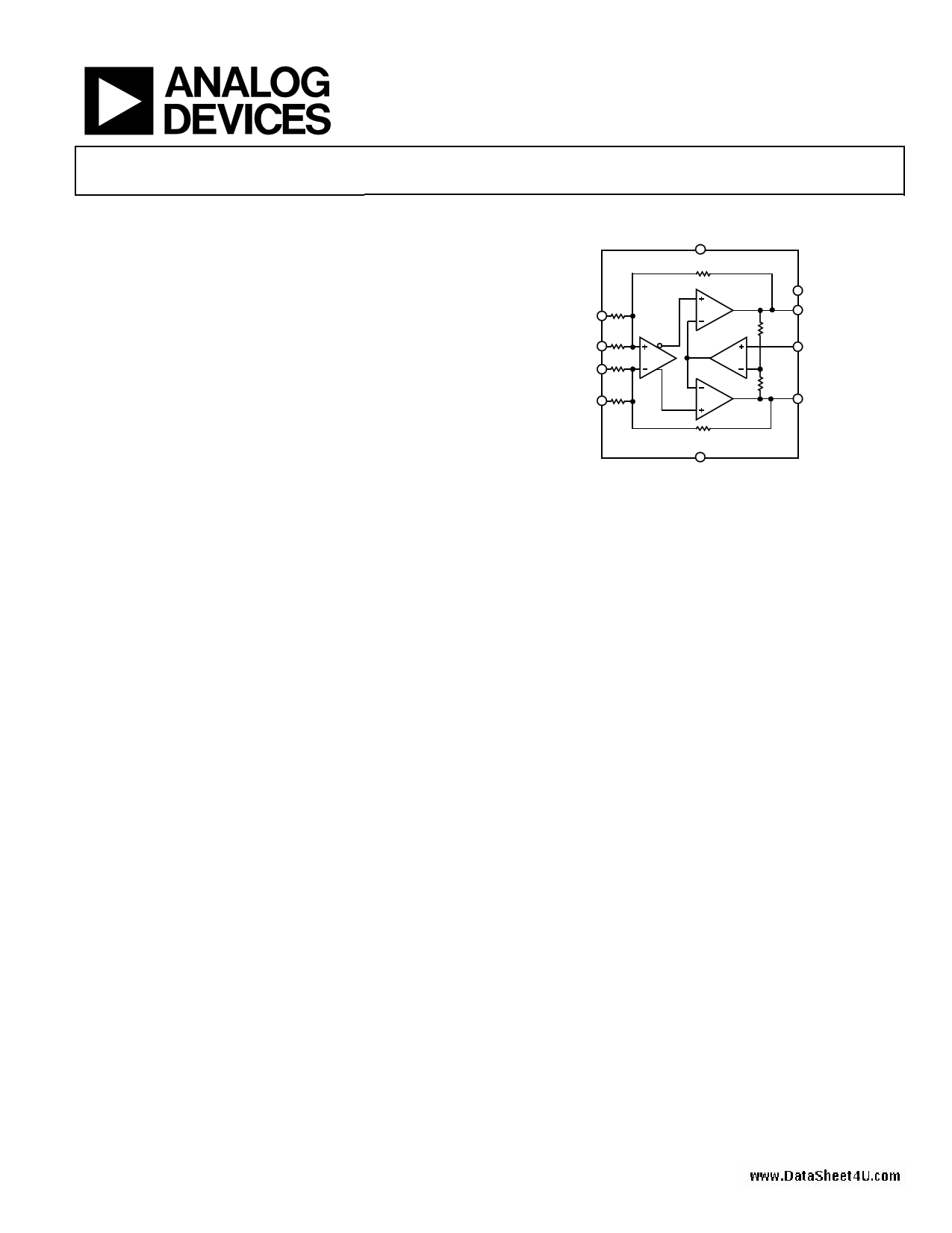
FUNCTIONAL BLOCK DIAGRAM
VCC
RF
VIP2
VIP1
VIN1
VIN2
RG2
RG1
RG1
RG2
ENBL
VON
VCOM
VOP
RF ADL5562
GND
Figure 1.
The device is optimized for wideband, low distortion perform-
ance. These attributes, together with its adjustable gain
capability, make this device the amplifier of choice for general-
purpose IF and broadband applications where low distortion,
noise, and power are critical. This device is optimized for the
best combination of slew speed, bandwidth, and broadband
distortion. These attributes allow it to drive a wide variety of
ADCs and make it ideally suited for driving mixers, pin diode
attenuators, SAW filters, and multielement discrete devices.
Fabricated on an Analog Devices, Inc., high speed SiGe process,
the ADL5562 is supplied in a compact 3 mm × 3 mm, 16-lead
LFCSP package and operates over the temperature range of
−40°C to + 85°C.
Rev. 0
Information furnished by Analog Devices is believed to be accurate and reliable. However, no
responsibility is assumed by Analog Devices for its use, nor for any infringements of patents or other
rights of third parties that may result from its use. Specifications subject to change without notice. No
license is granted by implication or otherwise under any patent or patent rights of Analog Devices.
Trademarksandregisteredtrademarksarethepropertyoftheirrespectiveowners.
One Technology Way, P.O. Box 9106, Norwood, MA 02062-9106, U.S.A.
Tel: 781.329.4700
www.analog.com
Fax: 781.461.3113
©2009 Analog Devices, Inc. All rights reserved.
1 page 
www.DataSheet4U.com
ADL5562
Parameter
Conditions
Min Typ
Max Unit
250 MHz NOISE/HARMONIC PERFORMANCE
Second/Third Harmonic Distortion
AV = 6 dB, RL = 200 Ω, VOUT = 2 V p-p
−98/−94
dBc
AV = 12 dB, RL = 200 Ω, VOUT = 2 V p-p
−74/−86
dBc
AV = 15.5 dB, RL = 200 Ω, VOUT = 2 V p-p
−74/−84
dBc
Output Third-Order Intercept/
AV = 12 dB, RL = 200 Ω, VOUT = 2 V p-p composite
Third-Order Intermodulation Distortion (2 MHz spacing)
+41/−87
dBm/dBc
AV = 15.5 dB, RL = 200 Ω, VOUT = 2 V p-p composite
(2 MHz spacing)
+40/−86
dBm/dBc
Noise Spectral Density (RTI)
AV = 6 dB
3.2 nV/√Hz
AV = 12 dB
2.2 nV/√Hz
AV = 15.5 dB
1.6 nV/√Hz
1 dB Compression Point (RTO)
AV = 6 dB
19.8 dBm
AV = 12 dB
19.3 dBm
AV = 15.5 dB
19.1 dBm
500 MHz NOISE/HARMONIC PERFORMANCE
Second/Third Harmonic Distortion
AV = 6 dB, RL = 200 Ω, VOUT = 1 V p-p
−75/−69
dBc
AV = 12 dB, RL = 200 Ω, VOUT = 1 V p-p
−69/−73
dBc
AV = 15.5 dB, RL = 200 Ω, VOUT = 1 V p-p
−72/−75
dBc
Output Third-Order Intercept/
AV = 6 dB, RL = 200 Ω, VOUT = 1 V p-p composite
Third-Order Intermodulation Distortion (2 MHz spacing)
+40/−98
dBm/dBc
AV = 12 dB, RL = 200 Ω, VOUT = 1 V p-p composite
(2 MHz spacing)
+39/−97
dBm/dBc
AV = 15.5 dB, RL = 200 Ω, VOUT = 1 V p-p composite
(2 MHz spacing)
+38/−93
dBm/dBc
Noise Spectral Density (RTI)
AV = 6 dB
3.7 nV/√Hz
AV = 12 dB
2.2 nV/√Hz
AV = 15.5 dB
1.6 nV/√Hz
1 dB Compression Point (RTO)
AV = 6 dB
18.1 dBm
AV = 12 dB
18.1 dBm
AV = 15.5 dB
18.1 dBm
1000 MHz NOISE/HARMONIC PERFORMANCE
Second/Third Harmonic Distortion
AV = 6 dB, RL = 200 Ω, VOUT = 1 V p-p
−70/−60
dBc
AV = 12 dB, RL = 200 Ω, VOUT = 1 V p-p
−69/−61
dBc
AV = 15.5 dB, RL = 200 Ω, VOUT = 1 V p-p
−66/−59
dBc
Output Third-Order Intercept/
AV = 6 dB, RL = 200 Ω, VOUT = 1 V p-p composite
Third-Order Intermodulation Distortion (2 MHz spacing)
+24/−65
dBm/dBc
AV = 12 dB, RL = 200 Ω, VOUT = 1 V p-p composite
(2 MHz spacing)
+24/−66
dBm/dBc
AV = 15.5 dB, RL = 200 Ω, VOUT = 1 V p-p composite
(2 MHz spacing)
+25/−66
dBm/dBc
Noise Spectral Density (RTI)
AV = 6 dB
4.7 nV/√Hz
AV = 12 dB
2.2 nV/√Hz
AV = 15.5 dB
1.6 nV/√Hz
1 dB Compression Point (RTO)
AV = 6 dB
15 dBm
AV = 12 dB
15.1 dBm
AV = 15.5 dB
15.1 dBm
1 See the Applications Information section for a discussion of single-ended input, dc-coupled operation.
Rev. 0 | Page 5 of 24
5 Page 
www.DataSheet4U.com
–30 –60
–40
AAAVVV
MAXIMUM
MID
MINIMUM
–70
–50 –80
–60 –90
–70 –100
–80 –110
–90 –120
–100
0
–130
100 200 300 400 500 600 700 800 900 1000
RLOAD (Ω)
Figure 21. HD2/HD3 vs. Load
TIME (2.5ns/DIV)
Figure 22. ENBL Time Domain Response
2V p-p OUTPUT
TIME (2.5ns/DIV)
Figure 23. Large Signal Pulse Response, AV = 15.5 dB
ADL5562
–55 –60
–60
AAAVVV
MAXIMUM
MID
MINIMUM
–65
–65 –70
–70 –75
–75 –80
–80 –85
–85 –90
–90 –95
–95 –100
–100
–105
–105
–110
1.1 1.2 1.3 1.4 1.5 1.6 1.7 1.8 1.9
VCOM (V)
Figure 24. HD2/HD3 vs. VCOM
1.0 0
0.9
AAAVVV
MAXIMUM
MID
MINIMUM
–20
0.8 –40
0.7 –60
0.6 –80
0.5 –100
0.4 –120
0.3 –140
0.2 –160
0.1 –180
0 100 200 300 400 500 600 700 800 900 1000
FREQUENCY (MHz)
Figure 25. Group Delay and Phase vs. Frequency
110 80
100
RL = 1kΩ
AAAVVV
MAXIMUM
MID
MINIMUM
70
90 60
80
RL = 200Ω
70
50
40
60 30
50 20
40 10
30
10M
100M
0
1G
FREQUENCY (Hz)
Figure 26. Common-Mode Rejection Ratio vs. Frequency
Rev. 0 | Page 11 of 24
11 Page | ||
| Páginas | Total 24 Páginas | |
| PDF Descargar | [ Datasheet ADL5562.PDF ] | |
Hoja de datos destacado
| Número de pieza | Descripción | Fabricantes |
| ADL5561 | 2.9 GHz Ultralow Distortion RF/IF Differential Amplifier | Analog Devices |
| ADL5562 | 3.3 GHz Ultralow Distortion RF/IF Differential Amplifier | Analog Devices |
| ADL5565 | 6 GHz Ultrahigh Dynamic Range Differential Amplifier | Analog Devices |
| ADL5566 | Dual Differential Amplifier | Analog Devices |
| Número de pieza | Descripción | Fabricantes |
| SLA6805M | High Voltage 3 phase Motor Driver IC. |
Sanken |
| SDC1742 | 12- and 14-Bit Hybrid Synchro / Resolver-to-Digital Converters. |
Analog Devices |
|
DataSheet.es es una pagina web que funciona como un repositorio de manuales o hoja de datos de muchos de los productos más populares, |
| DataSheet.es | 2020 | Privacy Policy | Contacto | Buscar |