|
|
PDF R2051 Data sheet ( Hoja de datos )
| Número de pieza | R2051 | |
| Descripción | 2 wire interface Real-Time Clock ICs | |
| Fabricantes | RICOH electronics | |
| Logotipo |  |
|
Hay una vista previa y un enlace de descarga de R2051 (archivo pdf) en la parte inferior de esta página. Total 30 Páginas | ||
|
No Preview Available !
R2051 SERIES
2 wire interface Real-Time Clock ICs with Battery Backup switch-over Function
NO.EA-104-070626
OUTLINEwww.datasheet4u.com
The R2051 is a CMOS real-time clock IC connected to the CPU by two signal lines, SCL and SDA, and
configured to perform serial transmission of time and calendar data to the CPU. Further, battery backup switchover
circuit and a voltage detector are incorporated. The periodic interrupt circuit is configured to generate interrupt
signals with six selectable interrupts ranging from 0.5 seconds to 1 month. The 2 alarm interrupt circuits generate
interrupt signals at preset times. As the oscillation circuit is driven under constant voltage, fluctuation of the
oscillator frequency due to supply voltage is small, and the time keeping current is small (TYP. 0.4µA at 3V). The
oscillation halt sensing circuit can be used to judge the validity of internal data in such events as power-on; The
supply voltage monitoring circuit is configured to record a drop in supply voltage below two selectable supply
voltage monitoring threshold settings. The 32.768kHz clock output function (CMOS output) is intended to output
sub-clock pulses for the external microcomputer. The oscillation adjustment circuit is intended to adjust time counts
with high precision by correcting deviations in the oscillation frequency of the quartz crystal unit. Battery backup
switchover function is the automatic switchover circuit between a main power supply and a backup battery of
primary or secondary battery. Switchover is executed by monitoring the voltage of a main power supply, therefore
the voltage of a backup battery voltage is not relevant. Since the package for these ICs is SSOP16 (5.0x6.4x1.25:
R2051Sxx), FFP12 (2.0x2.0x1.0: R2051Kxx), or TSSOP10G (4.0x2.9x1.0: R2051Txx), high density mounting of
ICs on boards is possible.
FEATURES
• Minimum Timekeeping supply voltage Typ. 0.75V (Max. 1.00V); VDD pin
• Low power consumption 0.4µA TYP (1.0µA MAX.) at VDD=3V
• Built-in Backup switchover circuit (can be used for a primary battery, a secondary battery, or an electric double
layer capacitor)
• Only two signal lines (SCL and SDA) required for connection to the CPU. ( I2C-Bus Interface, 400kHz)
• Time counters (counting hours, minutes, and seconds) and calendar counters (counting years, months, days,
and weeks) (in BCD format)
• Interrupt circuit configured to generate interrupt signals (with interrupts ranging from 0.5 seconds to 1 month)
to the CPU and provided with an interrupt flag and an interrupt halt (except R2051Txx)
• 2 alarm interrupt circuits (Alarm_W for week, hour, and minute alarm settings and Alarm_D for hour and
minute alarm settings) (except R2051Txx)
• Built-in voltage detector with delay
• With Power-on flag to prove that the power supply starts from 0V
• 32-kHz clock output pin (CMOS output. “H” level is always equal to VCC.)
• Supply voltage monitoring circuit with two supply voltage monitoring threshold settings
• Automatic identification of leap years up to the year 2099
• Selectable 12-hour and 24-hour mode settings
• High precision oscillation adjustment circuit
• Built-in oscillation stabilization capacitors (CG and CD)
• CMOS process
• Package SSOP16 (5.0mm x 6.4mm x 1.25mm : R2051Sxx), FFP12 (2.0mm x 2.0mm x 1.0mm : R2051Kxx)
TSSOP10G (4.0x2.9x1.0: R2051Txx)
1
1 page 
R2051 Series
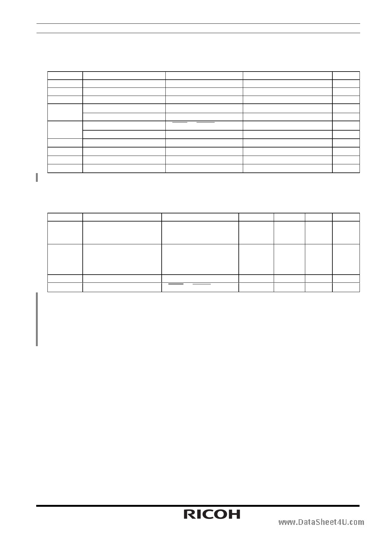
ABSOLUTE MAXIMUM RATINGS
(VSS=0V)
Symbol
Item
VCC Supply Voltage 1
www.datasheeVt4DuD.com
VSB
Supply Voltage 2
Supply Voltage 3
VI Input Voltage 1
Input Voltage 2
VO Output Voltage 1
IOUT
PD
Topt
Tstg
Output Voltage 2
Maximum Output Current
Power Dissipation
Operating Temperature
Storage Temperature
*1) Except R2051Txx
Pin Name
VCC
VDD
VSB
SCL, SDA
CIN
INTR , VDCC *1)
CLKOUT
VDD
Topt = +25°C
Description
-0.3 to +6.5
-0.3 to +6.5
-0.3 to +6.5
-0.3 to +6.5
-0.3 to VDD+0.3
-0.3 to +6.5
-0.3 to VCC+0.3
10
300
-40 to +85
-55 to +125
Unit
V
V
V
V
V
V
V
mA
mW
°C
°C
RECOMMENDED OPERATING CONDITIONS
Symbol
Item
Vaccess Supply Voltage
VCLK Minimum Timekeeping
Voltage
CGout,CDout=0pF
*2), *3)
fXT Oscillation Frequency
VPUP
Pull-up Voltage
Pin Name
VCC power supply
voltage for interfacing
with CPU
INTR , VDCC *4)
(VSS=0V, Topt=-40 to +85°C)
Min,
Typ. Max. Unit
-VDET1
5.5 V
*1)
0.75
1.00 V
32.768
5.5
kHz
V
*1) -VDET1 in Vaccess specification is guaranteed by design.
*2) CGout is connected between OSCIN and VSS, CDout is connected between OSCOUT and VSS.
R2051 series incorporates the capacitors between OSCIN and VSS, between OSCOUT and VSS.
Then normally, CGout and CDout are not necessary.
*3) Quartz crystal unit: CL=6-8pF, R1=30KΩ
*4) Except R2051Txx
5
5 Page 
PACKAGE DIMENSIONS
• R2051Kxx
www.datasheet4u.com
9
10
7
6
1PIN INDEX
12
1
4
3
2PIN INDEX
0.35
0.2±0.15
(BOTTOM VIEW)
0.17±0.1
0.27±0.15
2.0±0.1
R2051 Series
0.05
0.35
0.25
1.0Max
unit: mm
11
11 Page | ||
| Páginas | Total 30 Páginas | |
| PDF Descargar | [ Datasheet R2051.PDF ] | |
Hoja de datos destacado
| Número de pieza | Descripción | Fabricantes |
| R2051 | 2 wire interface Real-Time Clock ICs | RICOH electronics |
| Número de pieza | Descripción | Fabricantes |
| SLA6805M | High Voltage 3 phase Motor Driver IC. |
Sanken |
| SDC1742 | 12- and 14-Bit Hybrid Synchro / Resolver-to-Digital Converters. |
Analog Devices |
|
DataSheet.es es una pagina web que funciona como un repositorio de manuales o hoja de datos de muchos de los productos más populares, |
| DataSheet.es | 2020 | Privacy Policy | Contacto | Buscar |
