|
|
|
PDF NCP1252 Data sheet ( Hoja de datos )
| Número de pieza | NCP1252 | |
| Descripción | Current Mode PWM Controller | |
| Fabricantes | ON Semiconductor | |
| Logotipo | ||
Hay una vista previa y un enlace de descarga de NCP1252 (archivo pdf) en la parte inferior de esta página. Total 20 Páginas | ||
|
No Preview Available !
NCP1252
Current Mode PWM
Controller for Forward and
Flyback Applications
The NCP1252 controller offers everything needed to build cost−
effective and reliable ac−dc switching supplies dedicated to ATX
power supplies. Thanks to the use of an internally fixed timer,
NCP1252 detects an output overload without relying on the auxiliary
Vcc. A Brown−Out input offers protection against low input voltages
and improves the converter safety. Finally a SOIC−8 package saves
PCB space and represents a solution of choice in cost sensitive project.
Features
• Peak Current Mode Control
• Adjustable Switching Frequency up to 500 kHz
• Jittering Frequency ±5% of the Switching Frequency
• Latched Primary Over Current Protection with 10 ms Fixed Delay
• Delay Extended to 150 ms in E Version
• Delayed Operation Upon Start−up via an Internal Fixed Timer
(A, B and C versions only)
• Adjustable Soft−start Timer
• Auto−recovery Brown−Out Detection
• UC384X−like UVLO Thresholds
• Vcc Range from 9 V to 28 V with Auto−recovery UVLO
• Internal 160 ns Leading Edge Blanking
• Adjustable Internal Ramp Compensation
• +500 mA / –800 mA Source / Sink Capability
• Maximum 50% Duty Cycle: A Version
• Maximum 80% Duty Cycle: B Version
• Maximum 65% Duty Cycle: C Version
• Maximum 47.5% Duty Cycle: D & E Versions
• Ready for Updated No Load Regulation Specifications
• SOIC−8 and PDIP−8 Packages
• These are Pb−Free Devices
Typical Applications
• Power Supplies for PC Silver Boxes, Games Adapter...
• Flyback and Forward Converter
www.onsemi.com
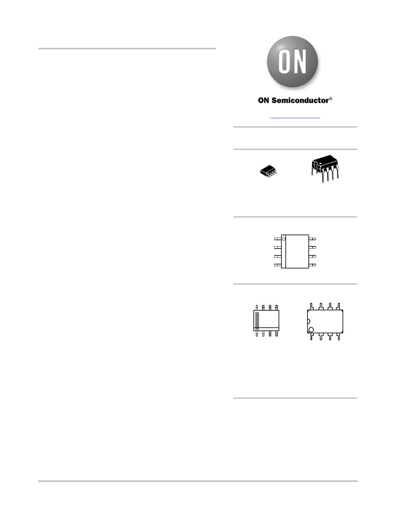
OFFLINE CONTROLLER
8
1
SOIC−8
CASE 751
SUFFIX D
PDIP−8
CASE 626
SUFFIX P
PIN CONNECTIONS
FB 1
BO
CS
RT
SS
VCC
DRV
GND
(Top View)
MARKING DIAGRAMS
8
1252x
ALYWX
G
1
1252AP
AWL
YYWWG
x = A, B, C, D or E
A = Assembly Location
L, WL = Wafer Lot
Y, YY = Year
W, WW = Work Week
G or G = Pb−Free Package
ORDERING INFORMATION
See detailed ordering and shipping information in the package
dimensions section on page 18 of this data sheet.
© Semiconductor Components Industries, LLC, 2016
January, 2016 − Rev. 7
1
Publication Order Number:
NCP1252/D
1 page 
NCP1252
Table 3. ELECTRICAL CHARATERISTICS
(VCC = 15 V, RT = 43 kW, CDRV = 1 nF. For typical values TJ = 25°C, for min/max values TJ = –25°C to +125°C, unless otherwise noted)
Characteristics
Test Condition
Symbol Min Typ Max Unit
DRIVE OUTPUT
Output voltage fall−time
VCC = 15 V, CDRV = 1 nF, tf − 22 − ns
90 to 10%
Clamping voltage (maximum gate voltage)
High−state voltage drop
CYCLE SKIP
VCC = 25 V
RDRV = 47 kW, CDRV = 1 nF
VCL
VCC = VCC(min) + 100 mV, RDRV VDRV(clamp)
= 47 kW, CDRV = 1 nF
−
−
15 18 V
50 500 mV
Skip cycle level
Skip threshold Reset
Skip threshold Hysteresis
SOFT START
Vskip
Vskip(reset)
Vskip(HYS)
0.2 0.3 0.4
− Vskip+ −
Vskip(HY
S)
− 25 −
V
V
mV
Soft−start charge current
SS pin = GND
ISS 8.8 10 11 mA
Soft start completion voltage threshold
VSS 3.5 4.0 4.5 V
Internal delay before starting the Soft start when
For A, B and C versions only
SSdelay
100
120
155 ms
VCC(on) is reached
− No delay for D & E versions
PROTECTION
Current sense fault voltage level triggering the
timer
FCS 0.9 1 1.1 V
Timer delay before latching a fault (overload or
short circuit) − A/B/C/D versions
When CS pin > FCS
Tfault
10 15 20 ms
Timer delay before latching a fault (overload or
short circuit) − E version
When CS pin > FCS
Tfault
120 155 200 ms
Brown−out voltage
Internal current source generating the Brown−out
hysteresis
3. Guaranteed by design
4. Vramp, Rramp Guaranteed by design
−5°C ≤ TJ ≤ +125°C
−25°C ≤ TJ ≤ +125°C
VBO 0.974 1 1.026 V
IBO 8.8 10 11.2 mA
8.6 10 11.2
Table 4. SELECTION TABLE
NCP1252
Start−up Delay
A Yes
B Yes
C Yes
D No
E No
Duty Ratio Max
50%
80%
65%
47.5%
47.5%
VCC Start (Typ.)
10 V
10 V
10 V
14 V
14 V
Fault Timer (Typ.)
15 ms
15 ms
15 ms
15 ms
150 ms
Fault
Latched
Latched
Latched
Latched
Latched
www.onsemi.com
5
5 Page 
NCP1252
Application Information
Introduction
The NCP1252 hosts a high−performance current−mode
controller specifically developed to drive power supplies
designed for the ATX and the adapter market:
• Current Mode operation: implementing peak
current−mode control topology, the circuit offers
UC384X−like features to build rugged power supplies.
• Adjustable switching frequency: a resistor to ground
precisely sets the switching frequency between 50 kHz
and a maximum of 500 kHz. There is no
synchronization capability.
• Internal frequency jittering: Frequency jittering
softens the EMI signature by spreading out peak energy
within a band ±5% from the center frequency.
• Wide Vcc excursion: the controller allows operation
up to 28 V continuously and accepts transient voltage
up to 30 V during 10 ms with IVCC < 20 mA
• Gate drive clamping: a lot of power MOSFETs do not
allow their driving voltage to exceed 20 V. The
controller includes a low−loss clamping voltage which
prevents the gate from going beyond 15 V typical.
• Low startup−current: reaching a low no−load standby
power represents a difficult exercise when the
controller requires an external, lossy, resistor connected
to the bulk capacitor. The start−up current is guaranteed
to be less than 100 mA maximum, helping the designer
to reach a low standby power level.
• Short−circuit protection: by monitoring the CS pin
voltage when it exceeds 1 V (maximum peak current),
the controller detects a fault and starts an internal
digital timer. On the condition that the digital timer
elapses, the controller will permanently latch−off. This
allows accurate overload or short−circuit detection
which is not dependant on the auxiliary winding. Reset
occurs when: a) a BO reset is sensed, b) VCC is cycled
down to VCC(min) level. If the short circuit or the fault
disappear before the fault timer ends, the fault timer is
reset only if the CS pin voltage level is below 1 V at
least during 3 switching frequency periods. This delay
before resetting the fault timer prevents any false or
missing fault or over load detection.
• Adjustable soft−start: the soft−start is activated upon
a start−up sequence (VCC going−up and crossing
VCC(on)) after a minimum internal time delay of 120 ms
(SSdelay). But also when the brown−out pin is reset
without in that case timer delay. This internal time
delay gives extra time to the PFC to be sure that the
output PFC voltage is in regulation. The soft start pin is
grounded until the internal delay is ended. Please note
that SSdelay is present only for A, B and C versions.
• Shutdown: if an external transistor brings the BO pin
down, the controller is shut down, but all internal
biasing circuits are alive. When the pin is released, a
new soft−start sequence takes place.
• Brown−Out protection: BO pin permanently monitors
a fraction of the input voltage. When this image is
below the VBO threshold, the circuit stays off and does
not switch. As soon the voltage image comes back
within safe limits, the pulses are re−started via a
start−up sequence including soft−start. The hysteresis is
implemented via a current source connected to the BO
pin; this current source sinks a current (IBO) from the
pin to the ground. As the current source status depends
on the brown−out comparator, it can easily be used for
hysteresis purposes. A transistor pulling down the BO
pin to ground will shut−off the controller. Upon release,
a new soft−start sequence takes place.
• Internal ramp compensation: a simple resistor
connected from the CS pin to the sense resistor allows
the designer to inject ramp compensation inside his
design.
• Skip cycle feature: When the power supply loads are
decreasing to a low level, the duty cycle also decreases
to the minimum value the controller can offer. If the
output loads disappear, the converter runs at the
minimum duty cycle fixed by the propagation delay and
driving blocks. It often delivers too much energy to the
secondary side and it trips the voltage supervisor. To
avoid this problem, the FB is allowed to impose the min
tON down to ~ Vf and it further decreases down to
Vskip, zero duty cycle is imposed. This mode helps to
ensure no−load outputs conditions as requested by
recently updated ATX specifications. Please note that
the converter first goes to min tON before going to zero
duty cycle: normal operation is thus not disturbed. The
following figure illustrates the different mode of
operation versus the FB pin level.
www.onsemi.com
11
11 Page | ||
| Páginas | Total 20 Páginas | |
| PDF Descargar | [ Datasheet NCP1252.PDF ] | |
Hoja de datos destacado
| Número de pieza | Descripción | Fabricantes |
| NCP1250 | Current-Mode PWM Controller | ON Semiconductor |
| NCP1251 | Current-Mode PWM Controller | ON Semiconductor |
| NCP1252 | Current Mode PWM Controller | ON Semiconductor |
| NCP1253 | Current-Mode PWM Controller | ON Semiconductor |
| Número de pieza | Descripción | Fabricantes |
| SLA6805M | High Voltage 3 phase Motor Driver IC. |
Sanken |
| SDC1742 | 12- and 14-Bit Hybrid Synchro / Resolver-to-Digital Converters. |
Analog Devices |
|
DataSheet.es es una pagina web que funciona como un repositorio de manuales o hoja de datos de muchos de los productos más populares, |
| DataSheet.es | 2020 | Privacy Policy | Contacto | Buscar |