|
|
|
PDF KH600 Data sheet ( Hoja de datos )
| Número de pieza | KH600 | |
| Descripción | Differential Input/Output Amplifier | |
| Fabricantes | Cadeka | |
| Logotipo | ||
Hay una vista previa y un enlace de descarga de KH600 (archivo pdf) en la parte inferior de esta página. Total 13 Páginas | ||
|
No Preview Available !
www.cadeka.com
KH600
1GHz, Differential Input/Output Amplifier
www.datasheet4u.com
Features
• DC - 1GHz bandwidth
• Fixed 14dB (5V/V) gain
• 100Ω (differential) inputs and outputs
• -74/-64dBc 2nd/3rd HD at 50MHz
• 45mA output current
• 9Vpp into 100Ω differential load
• 13,000V/µs slew rate
• Optional supply current and offset voltage adjustment
Description
The KH600 is the first amplifier to combine differential input
and output with a bandwidth of DC-1GHz at 2Vpp. The
inputs and outputs are 100Ω differential (50Ω single ended).
The KH600 operates from ±5V supplies and offers a fixed
gain of 14dB (5V/V).
The KH600 also offers optional supply current, differential
output offset voltage, and common mode offset voltage
adjustments.
Applications
• ATE systems
• High-end instrumentation
• High bandwidth output amplifier
• Differential buffer
• Line driver
The KH600 is constructed using Cadeka's in-house thin film
resistor/bipolar transistor technology. The KH600 is available
in a 12-pin TO-8 package.
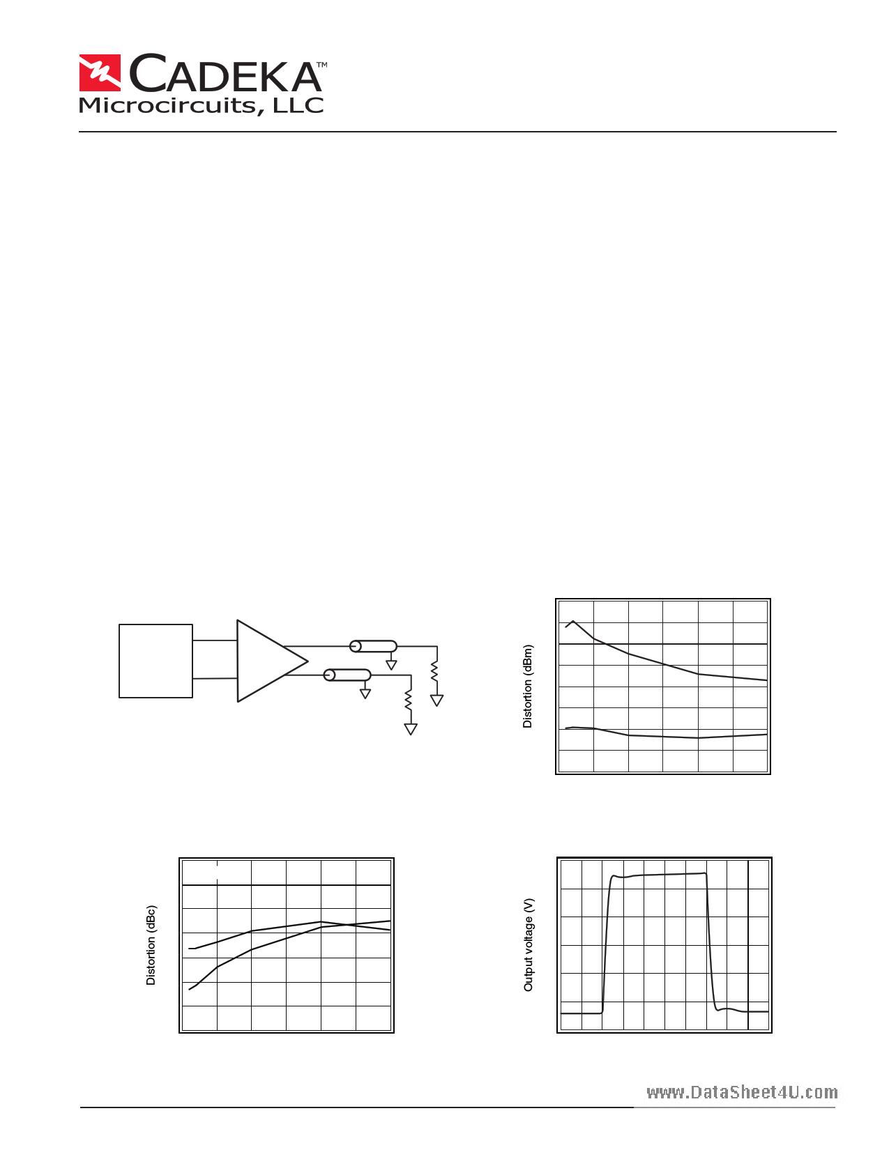
Typical Application
Differential
100Ω
Source
+
-
The KH600 includes 50Ω resistors from each
input to ground (resulting in a differential input
impedance of 100Ω).
50Ω
50Ω
Single Tone Intercept Point
100
90
80
I2
70
60
50
40
I3
30
20
0
50 100 150 200 250 300 350
Frequency (MHz)
2nd and 3rd Harmonic Distortion
-30
Vo = 2Vpp
-40
-50
-60
3rd
-70
2nd
-80
-90
-100
0
50 100 150 200 250
Frequency (MHz)
300
5Vpp Pulse Response
3
2
1
0
-1
-2
-3
Time (2ns/div)
REV. 2 January 2004
1 page 
KH600
DATA SHEET
Typical Operating Characteristics
(G = +5V/V (14dB), RL = 100Ω (differential), Ta = +25°C, +Vb1 = +Vb2 = +Vs = +5V, -Vb = -Vs = -5V; unless noted)
www.datasheet4u.com
2 Tone 3rd Order Intermod. Distortion
20
Vo = 5Vpp
0
-20
-40
-60
-80
-100
49.45
49.65 49.85 50.05 50.25
Frequency (MHz)
50.45
2 Tone 3rd Order Intermod. Distortion
20
Vo = 5Vpp
0
-20
-40
-60
-80
-100
99.45
99.65 99.85 100.05 100.25 100.45
Frequency (MHz)
2nd Harmonic Distortion vs. Vo
-30
-40
Vo = 5Vpp
-50
Vo = 2Vpp
-60
-70
Vo = 0.5Vpp
-80
-90 Vo = 1Vpp
-100
0
50 100 150 200 250
Frequency (MHz)
300
3rd Harmonic Distortion vs. Vo
-30
-40 Vo = 5Vpp
-50 Vo = 2Vpp
-60
Vo = 1Vpp
-70
-80
Vo = 0.5Vpp
-90
-100
0
50 100 150 200 250
Frequency (MHz)
300
Single Tone Intercept Point
100
90
80
I2
70
60
50
40
I3
30
20
0
50 100 150 200 250 300 350
Frequency (MHz)
-1dB Compression
24
23
22
21
20
19
18
17
16
0
100 200 300 400
Frequency (MHz)
500
Vs Supply Currents vs. Temperature
72
70
68
+Vs
66
64 -Vs
62
60
58
-40 -20 0 20 40 60
Temperature (°C)
80
Vb Supply Currents vs. Temperature
24
23
22
-Vb
21
+Vb1 shorted to +Vb2
20
19
18
-40 -20 0 20 40 60
Temperature (°C)
80
REV. 2 January 2004
5
5 Page 
KH600
DATA SHEET
changing the common mode from 1V to 3V set Vs = +7.5 and
-Vs to -3.5V. This example calls for a supply voltage of greater
than 10V. This will not effect supply current because as Figure 11
indicates, changing ±Vs has no effect on supply current.
-40
www.datasheet4u.co-m45
-50
-55
+Vs = +7.5V
-Vs = -3.5V
2Vpp, 50MHz
HD2
HD3
-60
HD3
-65
-70
HD2
-75
-80
01 23 4
Common Mode Output Voltage (V)
Figure 19: 2Vpp HD vs. Common Mode Voltage
-30
-35
+Vs = +7.5V
-Vs = -3.5V
-40 5Vpp, 50MHz
-45
HD3
HD2
-50
-55
-60
-65
-70
-75
-80
01 23 4
Common Mode Output Voltage (V)
Figure 20: 5Vpp HD vs. Common Mode Voltage
140
+Vs = +7.5V
-Vs = -3.5V
120
100
Is, -Is
80
Layout Considerations
General layout and supply bypassing play major roles in high
frequency performance. Cadeka has evaluation boards to use
as a guide for high frequency layout and as aid in device testing
and characterization. Follow the steps below as a basis for
high frequency layout:
• Include all recommended 6.8µF and 0.01µF
bypass capacitors
• Place the 6.8µF capacitors within 0.75 inches of
the power pin
• Place the 0.01µF capacitors within 0.1 inches of
the power pin
• Remove the ground plane under and around the part,
especially near the input and output pins to reduce
parasitic capacitance
• Minimize all trace lengths to reduce series inductances
• A 10pF to 50pF bypass capacitor can be used between
pins 5 and 6 and between pins 10 and 11 to reduce
crosstalk from the positive supply
Refer to the evaluation board layouts shown in Figure 22 for
more information.
Evaluation Board Information
The following evaluation boards are available to aid in the
testing and layout of this device:
Evaluation
Board
KEB007
KEB009
Description
Products
Basic KH600 Eval Bd
KH600 Eval Bd with offset and
Icc Adjust Option
KH600
KH600
Do not include capacitors C2, C3, C7, C11, and C12
that are shown on the KEB007 evaluation board. Evaluation
board schematics and layouts are shown in Figure 22. Refer
to the schematic shown in Figure 1 for the KEB007 board
and Figure 3 for the KEB009 board.
60
40
01 23 4
Common Mode Output Voltage (V)
Figure 21: Resulting Is and -Is
REV. 2 January 2004
11
11 Page | ||
| Páginas | Total 13 Páginas | |
| PDF Descargar | [ Datasheet KH600.PDF ] | |
Hoja de datos destacado
| Número de pieza | Descripción | Fabricantes |
| KH600 | Differential Input/Output Amplifier | Fairchild Semiconductor |
| KH600 | Differential Input/Output Amplifier | Cadeka |
| Número de pieza | Descripción | Fabricantes |
| SLA6805M | High Voltage 3 phase Motor Driver IC. |
Sanken |
| SDC1742 | 12- and 14-Bit Hybrid Synchro / Resolver-to-Digital Converters. |
Analog Devices |
|
DataSheet.es es una pagina web que funciona como un repositorio de manuales o hoja de datos de muchos de los productos más populares, |
| DataSheet.es | 2020 | Privacy Policy | Contacto | Buscar |