|
|
|
PDF CDK1300 Data sheet ( Hoja de datos )
| Número de pieza | CDK1300 | |
| Descripción | 250 MSPS ADC | |
| Fabricantes | Cadeka | |
| Logotipo | ||
Hay una vista previa y un enlace de descarga de CDK1300 (archivo pdf) en la parte inferior de esta página. Total 12 Páginas | ||
|
No Preview Available !
Data Sheet
Amplify the Human Experience
CDK1300
8-bit, 250 MSPS ADC with Demuxed Outputs
www.datasheet4u.com
features
n TTL/CMOS/PECL input logic compatible
n High conversion rate: 250 MSPS
n Single +5V power supply
n Very low power dissipation: 310mW
n 220MHz full power bandwidth
n Power-down mode
n +3.0V/+5.0V (LVCMOS) digital output
logic compatibility
n Single/demuxed output ports selectable
Applications
n RGB video processing
n Digital communications
n High-speed instrumentation
n Digital Sampling Oscilloscopes (DSO)
n Projection display systems
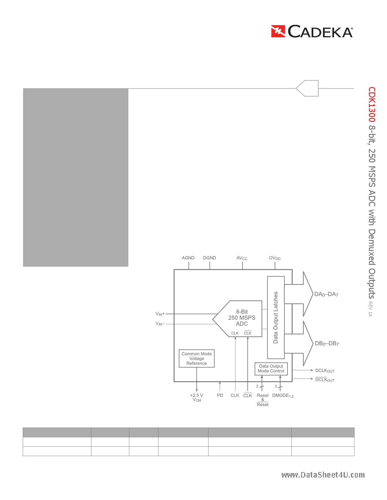
General Description
The CDK1300 is a high-speed, 8-bit analog-to-digital converter implemented
in an advanced BiCMOS process. An advanced folding and interpolating
architecture provides both a high conversion rate and very low power
dissipation of only 310mW. The analog inputs can be operated in
either single-ended or differential input mode. A 2.5V common mode
reference is provided on chip for the single-ended input mode to minimize
external components.
The CDK1300 digital outputs are demuxed (double-wide) with both dual-
channel and single-channel selectable output modes. Demuxed mode
supports either parallel aligned or interleaved data output. The output logic
is both +3.0V and +5.0V compatible. The CDK1300 is available in a 44-lead
TQFP surface mount package over the industrial temperature range of -40°C
to +85°C.
Block Diagram
Ordering Information
Part Number
CDK1300ITQ44
CDK1300ITQ44_Q
Package
TQFP-44
TQFP-44
Moisture sensitivity level for all parts is MSL-1.
Pb-Free
Yes
No
RoHS Compliant
Yes
No
Operating Temperature Range
-40°C to +85°C
-40°C to +85°C
Packaging Method
Rail
Rail
©2008 CADEKA Microcircuits LLC
www.cadeka.com
1 page 
Data Sheet
Electrical Characteristics
(TA = TMin to TMax, AVCC= +5V, OVDD = +5V, ƒclk = 250MHz, 50% duty cycle,
ƒIN = 70MHz, dual channel mode; unless otherwise noted)
Symbol Parameter
Conditions
Power Supply Requirements
wwwA.Vdcactasheet4u.Aconmalog Voltage Supply(2)
OVDD
Digital Voltage Supply(2)
AVcc
Current(1)
Power Dissipation(1)
Common Mode Reference Output
Voltage(1)
Voltage Tempco
Output Impedance
PSRR
Power Supply Rejection Ratio
Clock and Reset Inputs (Differential and Single-Ended)
VDIFF
Differental Signal Amplitude(1)
VIHD
Differental High Input Voltage(2)
VILD Differental Low Input Voltage(2)
VCMD
Differental Common Mode Input(2)
VIH Single-Ended High Input Voltage(2)
VIL Single-Ended Low Input Voltage(2)
IIH High Input Current(1)
IIL Low Input Current(1)
Power Down and Mode Control Inputs (Single-Ended)
High Input Voltage(2)
Low Input Voltage(2)
Max Input Current Low(1)
Max Input Current High <4.0V(1)
Digital Outputs
Logic “1“ Voltage(1)
Logic “0“ Voltage(1)
TR/TF Data
TR/TF DCLK
with Internal Voltage Reference
IOUT = ±50µA
VID = 1.5V
VID = 1.5V
IOH = -0.5mA
IOL = +1.6mA
OVDD = 3V, 10pF load
OVDD = 5V, 10pF load
OVDD = 3V, 10pF load
OVDD = 5V, 10pF load
Notes:
1. 100% production tested at +25°C.
2. Parameter is guaranteed (but not tested) by design and characterization data.
Min Typ Max Units
4.75 5.0 5.25
V
2.75 5.25 V
62 70 mA
310 350 mW
2.45 2.5 2.55
V
100 ppm/°C
1 kΩ
63 mV/V
400 mVpp
1.4 5 V
0 3.9 V
1.2 4.1 V
1.8 V
1.2 V
-100
20 +100 µA
-100
20 +100 µA
2.0
AVcc
V
0 1.0 V
-100
10 +100 µA
-100
10 +100 µA
OVDD-2.0 OVDD-0.06
0.13
3.5
2.0
1.3
0.7
0.2
V
V
ns
ns
ns
ns
©2008 CADEKA Microcircuits LLC
www.cadeka.com 5
5 Page 
Data Sheet
selected transformer does not exhibit core saturation at
the full-scale voltage. Proper termination of the input is
important for input signal purity. A small capacitor across
the input attenuates kickback noise from the internal track-
and-hold.
wwFwig.duarteas6heielltu4sut.craomtes a solution (based on operational ampli-
fiers) that can be used if a DC-coupled single-ended input
is desired.
Common-Mode Voltage Reference Circuit
The CDK1300 has an on-board common-mode voltage ref-
erence circuit (VCM). It is 2.5V and is capable of driving
50μA loads typically. The circuit is commonly used to drive
the center tap of the RF transformer in fully differential
applications. For single-ended applications, this output
can be used to provide the level shifting required for the
single-to-differential converter conversion circuit. Bypass
VCM to AGND by external 0.01μF capacitor, as shown in
Figure 3 on the previous page.
Clock Input
The clock input on the CDK1300 can be driven by either a
single-ended or double-ended clock circuit and can handle
TTL, PECL, and CMOS signals. When operating at high
sample rates it is important to keep the pulse width of the
clock signal as close to 50% as possible. For TTL/CMOS
single- ended clock inputs, the rise time of the signal
also becomes an important consideration.
Figure 6. DC-Coupled Single-Ended to Differential
Conversion (power supplies and bypassing are not shown)
Input Protection
All I/O pads are protected with an on-chip protection circuit.
This circuit provides ESD robustness and prevents latchup
under severe discharge conditions without degrading ana-
log transmission times.
Digital Outputs
The output circuitry of the CDK1300 has been designed
to be able to support three separate output modes. The
demuxed (double-wide) mode supports either parallel
aligned or interleaved data output. The single-channel mode
is not demuxed and can support direct output at speeds up
to 125 MSPS. The output format is straight binary (Table 1).
Power Supplies and Grounding
The CDK1300 is operated from a single power supply in
the range of 4.75V to 5.25V. Normal operation is suggest-
ed to be 5.0V. All power supply pins should be bypassed
as close to the package as possible. The analog and digital
grounds should be connected together with a ferrite bead
as shown in the typical interface circuit and as close to the
ADC as possible.
Power-Down Mode
To save on power, the CDK1300 incorporates a power-
down function. This function is controlled by the signal on
pin PD. When pin PD is set high, the CDK1300 enters the
power-down mode. All outputs are set to high impedance.
In the powerdown mode the CDK1300 dissipates 24mW
typically.
Table 1. Output Data Format
Analog Input
+FS
+FS - 1 LSB
+1 FS
-FS + 1 LSB
-FS
Output Code D7–D0
1111 1111
1111 111Ø
1000 000Ø
0000 000Ø
0000 0000
Ø indicates the flickering bit between logic 0 and 1
The data output mode is set using the DMODE1 and
DMODE2 inputs (pins 32 & 31 respectively). Table 2 describes
the mode switching options.
Table 2. Output Data Modes
Output Mode
Parallel Dual Channel Output
Interleaved Dual Channel Output
Single Channel Data Output
(Bank A only 125 MSPS max)
DMODE1
0
0
1
DMODE2
0
1
X
©2008 CADEKA Microcircuits LLC
www.cadeka.com 11
11 Page | ||
| Páginas | Total 12 Páginas | |
| PDF Descargar | [ Datasheet CDK1300.PDF ] | |
Hoja de datos destacado
| Número de pieza | Descripción | Fabricantes |
| CDK1300 | 250 MSPS ADC | Cadeka |
| CDK1301 | 250 MSPS A/D Converter | Cadeka |
| CDK1302 | Flash A/D Converter | Cadeka |
| CDK1303 | Flash A/D Converter | Cadeka |
| Número de pieza | Descripción | Fabricantes |
| SLA6805M | High Voltage 3 phase Motor Driver IC. |
Sanken |
| SDC1742 | 12- and 14-Bit Hybrid Synchro / Resolver-to-Digital Converters. |
Analog Devices |
|
DataSheet.es es una pagina web que funciona como un repositorio de manuales o hoja de datos de muchos de los productos más populares, |
| DataSheet.es | 2020 | Privacy Policy | Contacto | Buscar |