|
|
|
PDF CLC4050 Data sheet ( Hoja de datos )
| Número de pieza | CLC4050 | |
| Descripción | (CLCx050) Amplifiers | |
| Fabricantes | Cadeka | |
| Logotipo | ||
Hay una vista previa y un enlace de descarga de CLC4050 (archivo pdf) en la parte inferior de esta página. Total 17 Páginas | ||
|
No Preview Available !
Data Sheet
Amplify the Human Experience
Comlinear® CLC1050, CLC2050, CLC4050
Low Power, 3V to 36V, Single, Dual, Quad Amplifiers
www.datasheet4u.com
FEATURES
General Description
n Unity gain stable
n 100dB voltage gain
n 550kHz unity gain bandwidth
n 0.5mA supply current
n 20nA input bias current
n 2mV input offset voltage
n 3V to 36V single supply voltage range
The COMLINEAR CLC1050 (single), CLC2050 (dual), and CLC4050 (quad)
are voltage feedback amplifiers that are internally frequency compensated to
provide unity gain stability. At unity gain (G=1), these amplifiers offer 550kHz
of bandwidth. They consume only 0.5mA of supply current over the entire
power supply operating range. The CLC1050, CLC2050, and CLC4050 are
specifically designed to operate from single or dual supply voltages.
n ±1.5V to ±18V dual supply voltage range
n Input common mode voltage range
includes ground
n 0V to VS-1.5V output voltage swing
n CLC2050: improved replacement for
industry standard LM358
The COMLINEAR CLC1050, CLC2050, and CLC4050 offer a common mode
voltage range that includes ground and a wide output voltage swing. The
combination of low-power, high supply voltage range, and low supply current
make these amplifiers well suited for many general purpose applications and
as alternatives to several industry standard amplifiers on the market today.
n CLC4050: Improved replacement for
industry standard LM324
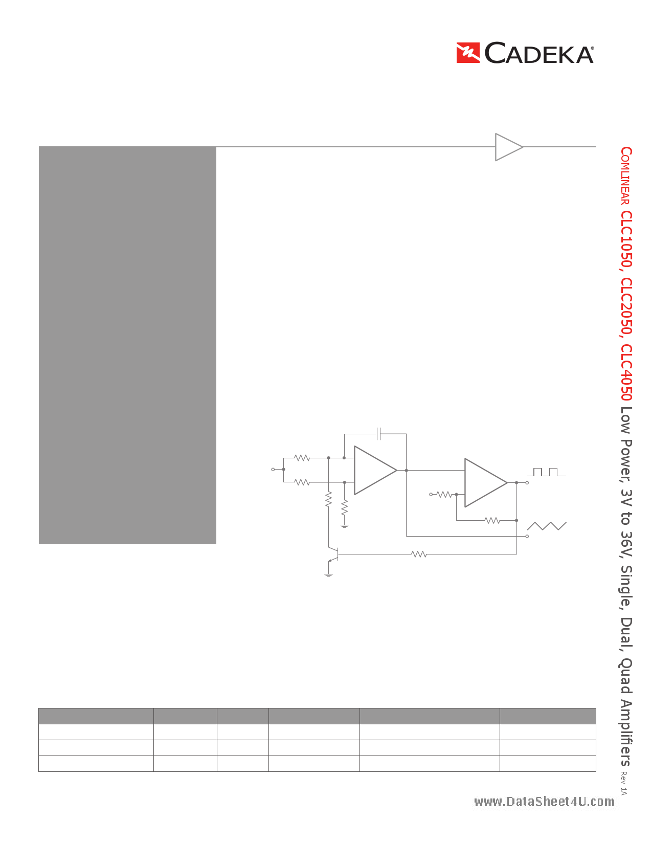
Typical Application - Voltage Controlled Oscillator (VCO)
n CLC1050: Pb-free SOT23-5
n CLC2050: Pb-free SOIC-8
n CLC4050: Pb-free SOIC-14
0.05µF
APPLICATIONS
n Battery Charger
n Active Filters
n Transducer amplifiers
n General purpose controllers
n General purpose instruments
R
VCC
100k
51k
R/2
50k
–
1/2
CLCx050
+
51k
51k
V+/2
–
1/2
CLCx050
+
100k
Output 1
Output 2
10k
Ordering Information
Part Number
Package
CLC1050IST5X
SOT23-5
CLC2050ISO8X
SOIC-8
CLC4050ISO14X
SOIC-14
Moisture sensitivity level for all parts is MSL-1.
Pb-Free
Yes
Yes
Yes
RoHS Compliant
Yes
Yes
Yes
Operating Temperature Range
-40°C to +85°C
-40°C to +85°C
-40°C to +85°C
Packaging Method
Reel
Reel
Reel
©2007-2009 CADEKA Microcircuits LLC
www.cadeka.com
1 page 
Data Sheet
Electrical Characteristics continued
TA = 25°C (if bold, TA = -40 to +85°C), Vs = +5V, -Vs = GND, Rf = Rg =2kΩ, RL = 2kΩ to VS/2, G = 2; unless otherwise
noted.
Symbol Parameter
Conditions
Min Typ Max Units
VOL Output Voltage Swing, Low (1)
www.datasheet4u.com
ISOURCE
Output Current, Sourcing (1)
ISINK
ISC
Output Current, Sinking (1)
Short Circuit Output Current (1)
+VS = 5V, RL = 10kΩ
5 20 mV
30 mV
20 40
VIN+ = 1V, VIN- = 0V, +VS = 15V, VOUT = 2V
20
mA
10 15
VIN+ = 0V, VIN- = 1V, +VS = 15V, VOUT = 2V
5
mA
VIN+ = 0V, VIN- = 1V, +VS = 15V, VOUT = 0.2V
12
50
μA
+VS = 15V
40 60 mA
Notes:
1. 100% tested at 25°C. (Limits over the full temperature range are guaranteed by design.)
2. The input common mode voltage of either input signal voltage should be kept > 0.3V at 25°C. The upper end of the common-mode voltage range is +VS - 1.5V at
25°C, but either or both inputs can go to +36V without damages, independent of the magnitude of VS.
©2007-2009 CADEKA Microcircuits LLC
www.cadeka.com 5
5 Page 
Data Sheet
(VLOAD)RMS = VPEAK / √2
( ILOAD)RMS = ( VLOAD)RMS / Rloadeff
The dynamic power is focused primarily within the output
stage driving the load. This value can be calculated as:
wwPwD.YdNaAtaMsIhCee=t4u(.VcoS+m - VLOAD)RMS × ( ILOAD)RMS
Assuming the load is referenced in the middle of the pow-
er rails or Vsupply/2.
Figure 4 shows the maximum safe power dissipation in
the package vs. the ambient temperature for the pack-
ages available.
2.5
SOIC-16
2
1.5 SOT23-6
1
0.5
0
-40
SOT23-5
-20 0
20 40 60
Ambient Temperature (°C)
80
CL (pF)
1nF
5nF
10nF
100
RS (Ω)
0
0
0
0
-3dB BW (kHz)
485
390
260
440
Table 1: Recommended RS vs. CL
For a given load capacitance, adjust RS to optimize the
tradeoff between settling time and bandwidth. In general,
reducing RS will increase bandwidth at the expense of ad-
ditional overshoot and ringing.
Overdrive Recovery
An overdrive condition is defined as the point when ei-
ther one of the inputs or the output exceed their specified
voltage range. Overdrive recovery is the time needed for
the amplifier to return to its normal or linear operating
point. The recovery time varies, based on whether the
input or output is overdriven and by how much the range
is exceeded. The CLCx050 will typically recover in less
than 30ns from an overdrive condition. Figure 6 shows the
CLC1050 in an overdriven condition.
Figure 4. Maximum Power Derating
Driving Capacitive Loads
Increased phase delay at the output due to capacitive load-
ing can cause ringing, peaking in the frequency response,
and possible unstable behavior. Use a series resistance, RS,
between the amplifier and the load to help improve stability
and settling performance. Refer to Figure 5.
Input
+
-
Rg
Rf
Rs Output
CL RL
4
3.5
3
Input
2.5
2
1.5
1
0.5
0
-0.5
0
20
Output
40 60
Time (us)
VIN = 1.25Vpp
G=5
4
3.5
3
2.5
2
1.5
1
0.5
0
-0.5
80 100
Figure 6. Overdrive Recovery
Figure 5. Addition of RS for Driving
Capacitive Loads
Table 1 provides the recommended RS for various capaci-
tive loads. The recommended RS values result in <=1dB
peaking in the frequency response. The Frequency Re-
sponse vs. CL plot, on page 6, illustrates the response of
the CLCx050.
©2007-2009 CADEKA Microcircuits LLC
www.cadeka.com 11
11 Page | ||
| Páginas | Total 17 Páginas | |
| PDF Descargar | [ Datasheet CLC4050.PDF ] | |
Hoja de datos destacado
| Número de pieza | Descripción | Fabricantes |
| CLC405 | Low-Cost/ Low-Power/ 110MHz Op Amp with Disable | National Semiconductor |
| CLC405 | CLC405 Low Cost Low Power 110MHz Op Amp with Disable (Rev. F) | Texas Instruments |
| CLC4050 | (CLCx050) Amplifiers | Cadeka |
| Número de pieza | Descripción | Fabricantes |
| SLA6805M | High Voltage 3 phase Motor Driver IC. |
Sanken |
| SDC1742 | 12- and 14-Bit Hybrid Synchro / Resolver-to-Digital Converters. |
Analog Devices |
|
DataSheet.es es una pagina web que funciona como un repositorio de manuales o hoja de datos de muchos de los productos más populares, |
| DataSheet.es | 2020 | Privacy Policy | Contacto | Buscar |