|
|
|
PDF LM22672 Data sheet ( Hoja de datos )
| Número de pieza | LM22672 | |
| Descripción | Step-Down Voltage Regulator | |
| Fabricantes | National Semiconductor Corporation | |
| Logotipo | ||
Hay una vista previa y un enlace de descarga de LM22672 (archivo pdf) en la parte inferior de esta página. Total 16 Páginas | ||
|
No Preview Available !
October 17, 2008
LM22672
1A SIMPLE SWITCHER®, Step-Down Voltage Regulator
www.dawtasihteeht4u.Fcoem atures
General Description
The LM22672 series of regulators are monolithic integrated
circuits which provide all of the active functions for a step-
down (buck) switching regulator capable of driving up to 1A
loads with excellent line and load regulation characteristics.
High efficiency (>90%) is obtained through the use of a low
ON-resistance N-channel MOSFET. The series consists of a
fixed 5V output and an adjustable version.
The SIMPLE SWITCHER® concept provides for an easy to
use complete design using a minimum number of external
components and National’s WEBENCH® design tool.
National’s WEBENCH® tool includes features such as exter-
nal component calculation, electrical simulation, thermal sim-
ulation, and Build-It boards for easy design-in. The switching
clock frequency is provided by an internal fixed frequency os-
cillator which operates at 500 kHz. The switching frequency
can also be adjusted with an external resistor or synchronized
to an external clock up to 1MHz. It is also possible to self-
synchronize multiple regulators to share the same switching
frequency. The LM22672 series also has built in thermal shut-
down, current limiting and an enable control input that can
power down the regulator to a low 25 µA quiescent current
standby condition. An adjustable soft-start feature is provided
by selecting an appropriate external soft-start capacitor.
Features
■ Wide input voltage range: 4.5V to 42V
■ Internally compensated voltage mode control
■ Stable with low ESR ceramic capacitors
■ 200 mΩ N-channel MOSFET
■ Output voltage options:
-ADJ (outputs as low as 1.285V)
-5.0 (output fixed to 5V)
■ ±1.5% feedback reference accuracy
■ Switching frequency of 500 kHz, adjustable between 200
kHz and 1 MHz
■ -40°C to 125°C operating junction temperature range
■ Precision enable pin
■ Integrated boot diode
■ Adjustable soft-start
■ Fully WEBENCH® enabled
■ Step-down and inverting buck-boost applications
Package
■ PSOP-8 (Exposed Pad)
Applications
■ Industrial Control
■ Telecom and Datacom Systems
■ Embedded Systems
■ Automotive Telematics and Body Electronics
■ Conversions from Standard 24V, 12V and 5V Input Rails
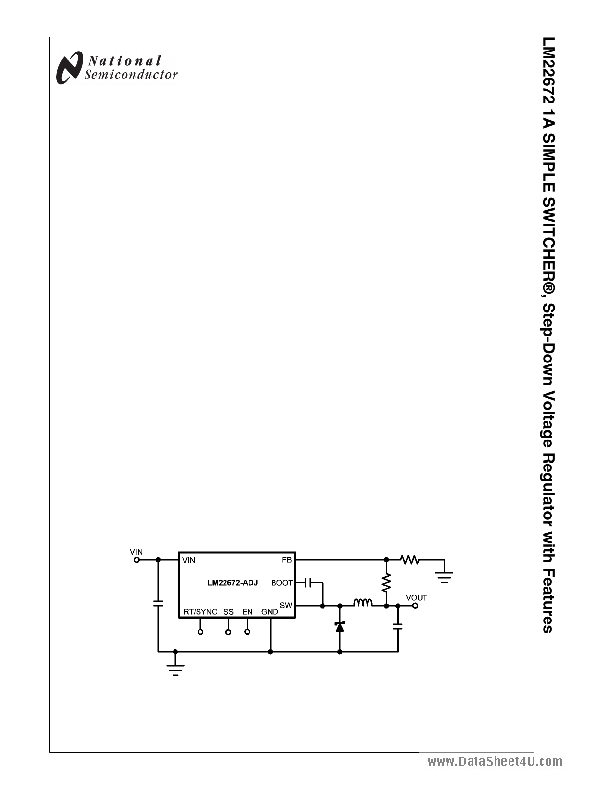
Simplified Application Schematic
© 2008 National Semiconductor Corporation 300767
30076701
www.national.com
1 page 
Feedback Bias Current vs Temperature
Normalized Enable Threshold Voltage vs Temperature
www.datasheet4u.com
30076705
Standby Quiescent Current vs Input Voltage
30076710
Normalized Feedback Voltage vs Temperature
30076706
Normalized Feedback Voltage vs Input Voltage
30076707
Switching Frequency vs RT/SYNC Resistor
30076709
5
30076713
www.national.com
5 Page 
input voltage transients are expected near the maximum rat-
ing of the LM22672, a careful evaluation of ringing and pos-
sible voltage spikes at the VIN pin should be completed. An
additional damping network or input voltage clamp may be
required in these cases.
Usually putting a higher ESR electrolytic input capacitor in
parallel to the low ESR bypass capacitor will help to reduce
excessive voltages during a line transient and will also move
the resonance frequency of the input filter away from the reg-
wwuwla.tdoar tbaashnedewti4duth.c.om
Output Capacitor
The output capacitor can limit the output ripple voltage and
provide a source of charge for transient loading conditions.
Multiple capacitors can be placed in parallel. Very low ESR
capacitors such as ceramic capacitors reduce the output rip-
ple voltage and noise spikes, while larger higher ESR capac-
itors in parallel provide large bulk capacitance for transient
loading conditions. An approximation for the output voltage
ripple is:
Where VFB = 1.285V typical for the -ADJ option and 5V for the
-5.0 option
30076723
FIGURE 4. Resistive Feedback Divider
where ΔIL is the inductor ripple current.
If the switching frequency is set higher than 500 kHz, the ca-
pacitance value may not be reduced accordingly due to sta-
bility requirements. The internal compensation is optimized
for circuits with a 500 kHz switching frequency. See the in-
ternal compensation section for more details.
Cboot Capacitor
The bootstrap capacitor between the BOOT pin and the SW
pin supplies the gate current to turn on the N-channel MOS-
FET. The recommended value of this capacitor is 10 nF and
should be a good quality, low ESR ceramic capacitor.
It is possible to put a small resistor in series with the Cboot
capacitor to slow down the turn-on transition time of the in-
ternal N-channel MOSFET. Resistors in the range of 10Ω to
50Ω can slow down the transition time. This can reduce EMI
of a switched mode power supply circuit. Using such a series
resistor is not recommended for every design since it will in-
crease the switching losses of the application and makes
thermal considerations more challenging.
Resistor Divider
For the -5.0 option no resistor divider is required for 5V output
voltage. The output voltage should be directly connected to
the FB pin. Output voltages above 5V can use the -5.0 option
with a resistor divider as an alternative to the -ADJ option.
This may offer improved loop bandwidth in some applications.
See the Internal Compensation section for more details.
For the -ADJ option no resistor divider is required for 1.285V
output voltage. The output voltage should be directly con-
nected to the FB pin. Other output voltages can use the -ADJ
option with a resistor divider.
The resistor values can be determined by the following equa-
tions:
-ADJ option:
-5.0 option:
A maximum value of 10 kΩ is recommended for the sum of
R1 and R2 to keep high output voltage accuracy for the –ADJ
option. A maximum of 2 kΩ is recommended for the -5.0 out-
put voltage option. For the 5V fixed output voltage option, the
total internal divider resistance is typically 9.93 kΩ.
At loads less than 5 mA, the boot capacitor will not hold
enough charge to power the internal high side driver. The
output voltage may droop until the boot capacitor is
recharged. Selecting a total feedback resistance to be below
3 kΩ will provide some minimal load and can keep the output
voltage from collapsing in such low load conditions.
Catch Diode
A Schottky type re-circulating diode is required for all
LM22672 applications. Ultra-fast diodes which are not Schot-
tky diodes are not recommended and may result in damage
to the IC due to reverse recovery current transients. The near
ideal reverse recovery characteristics and low forward volt-
age drop of Schottky diodes are particularly important diode
characteristics for high input voltage and low output voltage
applications common to the LM22672. The reverse recovery
characteristic determines how long the current surge lasts
each cycle when the N-channel MOSFET is turned on. The
reverse recovery characteristics of Schottky diodes mini-
mizes the peak instantaneous power in the switch occurring
during turn-on for each cycle. The resulting switching losses
are significantly reduced when using a Schottky diode. The
reverse breakdown rating should be selected for the maxi-
mum VIN, plus some safety margin. A rule of thumb is to select
a diode with the reverse voltage rating of 1.3 times the max-
imum input voltage.
The forward voltage drop has a significant impact on the con-
version efficiency, especially for applications with a low output
voltage. ‘Rated’ current for diodes varies widely from various
manufacturers. The worst case is to assume a short circuit
load condition. In this case the diode will carry the output cur-
rent almost continuously. For the LM22672 this current can
be as high as 1.5A (typical). Assuming a worst case 1V drop
across the diode, the maximum diode power dissipation can
be as high as 1.5W.
Circuit Board Layout
Board layout is critical for switching power supplies. First, the
ground plane area must be sufficient for thermal dissipation
11 www.national.com
11 Page | ||
| Páginas | Total 16 Páginas | |
| PDF Descargar | [ Datasheet LM22672.PDF ] | |
Hoja de datos destacado
| Número de pieza | Descripción | Fabricantes |
| LM22670 | LM22670/-Q1 42-V 3-A SIMPLE SWITCHER Step-Down Voltage Regulator With Features (Rev. P) | Texas Instruments |
| LM22670 | Step-Down Voltage Regulator | National Semiconductor Corporation |
| LM22670-Q1 | LM22670/-Q1 42-V 3-A SIMPLE SWITCHER Step-Down Voltage Regulator With Features (Rev. P) | Texas Instruments |
| LM22671 | LM22671/-Q1 42 V 500 mA SIMPLE SWITCHER Step-Down Voltage Regulator with Features (Rev. N) | Texas Instruments |
| Número de pieza | Descripción | Fabricantes |
| SLA6805M | High Voltage 3 phase Motor Driver IC. |
Sanken |
| SDC1742 | 12- and 14-Bit Hybrid Synchro / Resolver-to-Digital Converters. |
Analog Devices |
|
DataSheet.es es una pagina web que funciona como un repositorio de manuales o hoja de datos de muchos de los productos más populares, |
| DataSheet.es | 2020 | Privacy Policy | Contacto | Buscar |