|
|
PDF KESRX05 Data sheet ( Hoja de datos )
| Número de pieza | KESRX05 | |
| Descripción | 260 to 470MHz ASK Receiver | |
| Fabricantes | Zarlink Semiconductor | |
| Logotipo | ||
Hay una vista previa y un enlace de descarga de KESRX05 (archivo pdf) en la parte inferior de esta página. Total 28 Páginas | ||
|
No Preview Available !
www.DataSheet4U.com
This product is obsolete.
This information is available for your
convenience only.
For more information on
Zarlink’s obsolete products and
replacement product lists, please visit
http://products.zarlink.com/obsolete_products/
1 page 
KESRX05
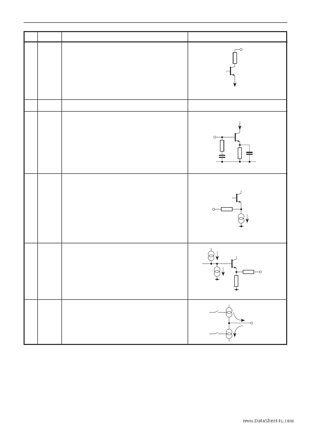
Pin Name
Function
9www.DRaFtaOSUheTet4U.cOomutput from internal RF amplifier
The RF amplifier has a high output impedance. The
internal 300Ω resistor is used to improve the ESD
protection of RFOUT.
Schematic
RFOP
300
10 VEERF
11 RFIN
For further information refer to the AC Electrical
Characteristics.
Negative supply for RF circuits
nternal input RF amplifier
To a first order approximation the input impedance
of the RF amplifier at UHF frequencies is set by the
internal bias resistor and capacitor network. Effects
of internal and external stray parasitics ignored.
For further information please refer to the AC
Electrical Characteristics.
240µA
(AGC OFF)
RFIN
1k
5p
240µA
830 10p
VEERF
12 AGC RF AGC time constant
The attack and decay time constant of the AGC is
set by the internal series resistor, current sink and
the external capacitor C8. Increasing the decay time
constant of the AGC circuit will impair the time to
good data of the receiver from power up PD0 to PD2.
AGC
360
6µA
For further information please refer to the IF Amp/
RSSI Detector section of the Functional Description.
13 PEAK Data signal peak detector output
The peak detector output is designed to be a low
impedance output. The peak detector monitors the
peak of the signal at pin 20 (DF2).
For further information please refer to the Baseband
section of the Functional Description.
300
190k
VEE
PEAK
14 DATAOP Sliced data output
The data output is the inverted sense of the input
signal at pin 20 (DF2) and is designed as a high im-
pedance output via two internal sink and source cur-
rent generators
HIGH
LOW
120µA
DATAOP
220µA
Table 1 Pin descriptions (continued)
Cont…
4
5 Page 
KESRX05
choice of bandwidth for the 10·7MHz ceramic filter depends
on frequency tolerancing of the transmitter, receiver, data
ratewwawn.dDactoamShpeoent4eUn.ctocmost.
The IF filter drive, IFOUT, is a voltage drive with a 300Ω
series resistance (see Table 1, pin 6). This allows
impedance matching to the ceramic IF filter to be set by
an external series resistor. A 10·7MHz ceramic filter with,
typically, a 300Ω input impedance does not require an
external matching resistor at IFOUT.
The input to the log amp, IFIN, is high impedance with an
internal 3kΩ shunt resistor. Impedance matching to the
output of the ceramic filter is achieved by an external shunt
resistor R9 between IFIN and IFDC1 (see Table 1, pin 3).
Phase Lock Loop VCO
The local oscillator (LO) is a VCO locked to a crystal
reference by a phase lock loop (PLL). The VCO gain is
nominally 26MHz/V depending on the external varactor
used. The LO frequency is divided by 64 and fed into the
phase-frequency detector, where the reference frequency
is provided from the crystal oscillator. The AC phase
detector output current into the PLL loop filter is nominally
615µA. The maximum loop filter bandwidth is 50kHz.
VCO Circuit Design and Layout
The Local Oscillator (LO) frequency is controlled by a
parallel resonant tuned circuit. The frequency of the local
oscillator is controlled by a Phase Locked Loop (PLL),
referenced to the crystal frequency.
Designing for VCO Track Parasitics
To remove the effect of track parasitics the following pro-
cedure should be adopted.
1. Open circuit the control feed back from the PLL con-
trol loop by removing R1.
2. Connect an external Power Supply Unit (PSU = VCC/ 2)
in place of R1, LF output (Figure 3).
3. Using a spectrum analyser, monitor the LO level at
the RFIN port. Alternatively use a small pick-up coil to
loosely couple to the signal generated across L2.
4. Note that the LO level is ,,265 dBm, range = 300 to
500MHz.
5. Vary the value of the PSU input to confirm that there is
a corresponding change in LO frequency. Set the PSU
at VCC/2. If the VCO does not oscillate at VCC/2, char-
acterise the LO at an alternative voltage.
6. Using a plot of the varactor characteristic determine
the varactor capacitance at VCC/2. e.g. for a 2V VCC
design the Siemens BB833 capacitance at 1V = 10pF
(approx.).
7. Using the following equation deduce the value of the
total stray parasitic capacitance CP.
@ #CP =
1
~2p3fLO23L2!2CV
where CV = varactor capacitance at VCC/2
8. Using the following equation select the nearest value
for L2 to centre the VCO at VCC/2.
L2
=
1
~2p3fLO2!3~CP1CV!
9. By varying the PSU voltage confirm that the LO is
centred correctly at VCC/2, and that the oscillator
operates over the range 0V to VCC.
10. Disconnect the PSU and reconnect R1. Measure the
value at LF output using a 310 probe and an
oscilloscope. This should be a direct voltage with no
ripple at VCC/2 (60.3V). If not repeat steps 1 to 8. To
compensate for non standard inductor values vary the
value of C18 and C11 to vary the capacitance of the
varactor to centre the VCC at VCC/2.
NOTE: It is important to minimise stray capacitance in
the VCO circuit to ensure that the VCO starts oscillat-
ing. The use of a varactor with a low capacitance at
zero bias is advisable. Similarly, reducing the values of
C11 and C18 whilst increasing L2 will help to reduce
the capacitance of the varactor at 0V, improving the re-
liability of the oscillator. A compact design methodology
is recommended for the VCO circuit components L2,
C11, C18 and D1.
10
11 Page | ||
| Páginas | Total 28 Páginas | |
| PDF Descargar | [ Datasheet KESRX05.PDF ] | |
Hoja de datos destacado
| Número de pieza | Descripción | Fabricantes |
| KESRX01 | 290 - 460MHz ASK Receiver | Zarlink Semiconductor Inc |
| KESRX04 | 260 to 470MHz. ASK Receiver with Power Down | Zarlink Semiconductor Inc |
| KESRX05 | 260 to 470MHz ASK Receiver | Zarlink Semiconductor |
| Número de pieza | Descripción | Fabricantes |
| SLA6805M | High Voltage 3 phase Motor Driver IC. |
Sanken |
| SDC1742 | 12- and 14-Bit Hybrid Synchro / Resolver-to-Digital Converters. |
Analog Devices |
|
DataSheet.es es una pagina web que funciona como un repositorio de manuales o hoja de datos de muchos de los productos más populares, |
| DataSheet.es | 2020 | Privacy Policy | Contacto | Buscar |
