|
|
|
PDF XC6419 Data sheet ( Hoja de datos )
| Número de pieza | XC6419 | |
| Descripción | Dual LDO Regulator | |
| Fabricantes | Torex Semiconductor | |
| Logotipo | ||
Hay una vista previa y un enlace de descarga de XC6419 (archivo pdf) en la parte inferior de esta página. Total 29 Páginas | ||
|
No Preview Available !
XC6419 Series
Duwawlw.LDaDtaOSheRet4eU.gcoumlator (ch1=300mA, ch2=100mA) with ON/OFF Switch
ETR0338-003
GENERAL DESCRIPTION
The XC6419 series is a dual CMOS LDO regulator. The series features high accuracy, low output noise, high
ripple rejection and low dropout and consists of a voltage reference, error amplifier, driver transistor, current limiter,
thermal shutdown circuit and phase compensation circuit. Each output voltage is set independently by laser
trimming and selectable in 0.05V increments within a range of 0.8 to 5.0V.
The EN function turns each output of the two regulators off independently. In this state, the electric charge at the
output capacitor (CL) is discharged via the internal auto-discharge switch, and as a result the VOUT voltage quickly
returns to the VSS level. The output stabilization capacitor (CL) is also compatible with low ESR ceramic
capacitors. The high level of output stability is maintained even during frequent load fluctuations, due to the
excellent transient response performance. VR1 and VR2 are completely isolated so that a cross talk during load
fluctuations is minimized.
APPLICATIONS
●Mobile phones
● Cordless phones, Wireless communication equipment
●Portable games
●Digital still cameras, Digital video cameras
●Portable audio equipment
● PDAs
■FEATURES
Input Voltage Range
Maximum Output Current
Output Voltage Range
Output Accuracy
Dropout Voltage
(VOUT=2.8V)
Low Power Consumption
Stand-by Current
Ripple Rejection
Current Limit
Low ESR Capacitor
CL High Speed Discharge
Small Packages
: 1.5~6.0V
: ch1.300mA / ch2.100mA
: 0.8~5.0V
: ±1% (XC6419A/B)
±20mA@ VOUT≦2.0V
±2% (XC6419C/D)
±30mA@ VOUT≦1.5V
:
ch1.115mV@IOUT=200mA
ch2.115mV@IOUT=50mA
: ch1.28μA / ch2.23μA
: Less than 0.1μA
: 60dB@f=1kHz
: ch1.400mA / ch2.150mA
: USP-6C, SOT-26
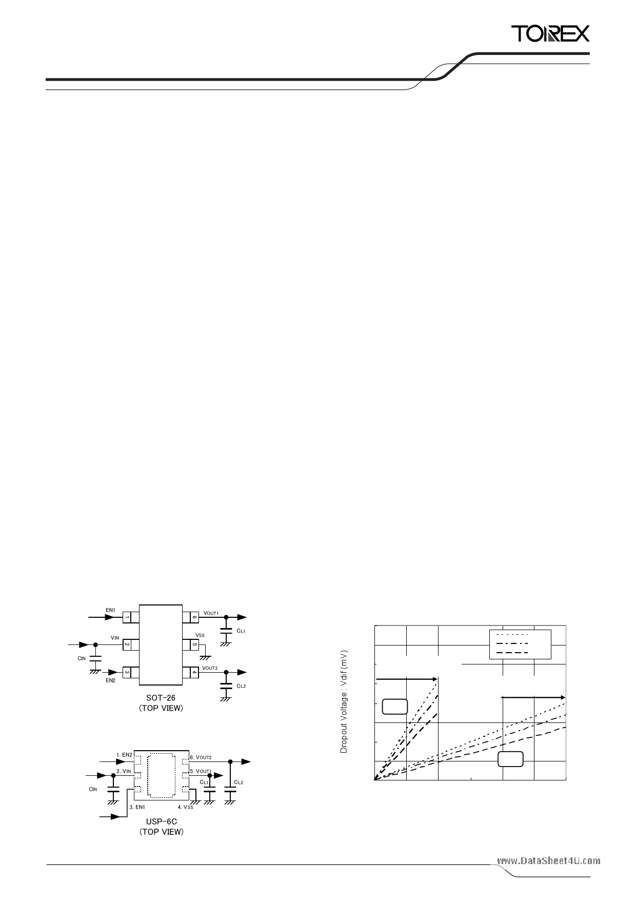
TYPICAL APPLICATION CIRCUITS
TYPICAL PERFORMANCE
CHARACTERISTICS
Dropout Voltage vs. Output Current
400
VOUVT=O2UT.8=V2.8V
85℃
350
300
ch22CHM最ax大imu出m力O電utp流ut Current
100mA
25℃
-40℃
250
ch1 Ma1xCimHu最m 大Ou出tpu力t C電urr流ent
300mA
200 2cCh2H
150
100
50 1cCh1H
0
0 50 100 150 200 250 300
OOuuttpuutCCuurrrreennt :: IOOUUTT [(mmA])
1/29
1 page 
XC6419
Series
ELECTRICAL CHARACTERISTICS (Continued)
www.DataSheet4U.com
XC6419 Series
Regulator 2
PARAMETER
Output Voltage
Output Current
Load Regulation
Dropout Voltage (*5)
Supply Current
Stand-by Current
Line Regulation
Input Voltage
Output Voltage
Temperature
Characteristics
Ripple Rejection Rate
Limit Current
Short Current
EN ”H” Level Voltage
EN ”L” Level Voltage
EN ”H” Level Current
EN ”L” Level Current
CL Discharge Resistor (*8)
SYMBOL
VOUT(E)
(*2)
IOUTMAX
ΔVOUT
Vdif
ISS
ISTBY
ΔVOUT
ΔVIN ・VOUT
VIN
ΔVOUT
ΔTa ・VOUT
PSRR
ILIM
ISHORT
VENH
VENL
IENH
IENL
RDCHG
CONDITIONS
VOUT(T)≧2.0V (A, B Series),
VEN2=VIN, IOUT=10mA
VOUT≦1.95V (A, B Series),
VEN2=VIN, IOUT=10mA
VOUT(T)>1.5V(C, D Series)
VEN2=VIN, IOUT=10mA
VOUT≦1.5V (C, D Series)
VEN2=VIN, IOUT=10mA
VEN2=VIN, 0.1mA≦IOUT≦50mA
IOUT=50mA, VEN2=VIN
VIN=VEN2=VOUT(T)+1.0V, IOUT=0mA
VIN=6.0V, VEN2=VSS
VOUT(T)+0.5V≦VIN≦6.0V
:VOUT(T)≧1.0V
VEN2=VIN, IOUT=10mA
1.5V≦VIN≦6.0V
:VOUT(T)≦0.95V
VEN2=VIN, IOUT=10mA
VEN2=VIN, IOUT=30mA
-40℃≦Ta≦85℃
VIN={VOUT(T)+1.0}
VDC+0.5Vp-pAC
:VOUT(T)≦4.75V
VEN2=VIN, IOUT=30mA、f=1kHz
VIN=5.75VDC+0.5Vp-pAC
:VOUT(T)≧4.8V
VEN2=VIN, IOUT=30mA, f=1kHz
VEN2=VIN
VEN2=VIN, Short VOUT to VSS level
VEN2=VIN
VEN2=VSS
VIN=6.0V, VOUT=4.0V, VEN2= VSS
MIN.
×0.99
(*3)
TYP.
MAX.
×1.01
(*3)
-0.02
(*3)
×0.98
(*3)
VOUT(T)
(*4)
+0.02
(*3)
×1.02
(*3)
-0.03
(*3)
+0.03
(*3)
100
Refer to table E-21
Refer to table E-22
23 60
0.01 0.1
0.01 0.20
1.5 6.0
±100
60
110 150
15
1.2 6.0
0.3
-0.1 0.1
-0.1 0.1
550
UNITS
V
mA
mV
mV
A
A
%/V
V
ppm/
dB
mA
mA
V
V
A
A
Ω
Ta=25℃
CIRCUITS
NOTE:
*1: Unless otherwise stated, VIN=VOUT (T) +1.0V, VEN1=0V.
*2: VOUT (E) is actual output voltage (refer to the voltage table)
(ie. The output voltage when “VOUT (T) +1.0V” is provided at the VIN pin while maintaining a certain IOUT value.
*3: Characteristics of the actual VOUT (E) by nominal output voltage is shown in the voltage table
*4: VOUT (T) is nominal output voltage
*5: Vdif = VIN1(*7) -VOUT3(*6)
*6: VOUT3 is a voltage equal to 98% of the output voltage whenever an amply stabilized IOUT{VOUT(T)+1.0V} is input.
*7: VIN1 is the input voltage when VOUT3 appears while input voltage is gradually decreased.
*8: For XC6419 xB/xD series only.
XC6419 xA /xC series discharge with only Rx1 and Rx2 resistors as shown in the BLOCK DIAGRAMS.
5/29
5 Page 
XC6419
Series
wTwYw.DPaItaCShAeeLt4UP.coEmRFORMANCE CHARACTERISTICS
* EN Voltage condition: Unless otherwise stated, VEN=VIN while the other channel is turned off ((VEN=VSS).
((11) ) 出Ou力tp電ut圧Vo-l出tag力e電vs流. O特u性tpu例t Current
XC6419(VOUT1=0.8V) VR1
XC6419(VOUT2=0.8V) VR2
Ta=25℃, CIN=1.0μF(ceramic), CL1=2.2μF(ceramic)
1.0
Ta=25℃, CIN=1.0μF(ceramic), CL2=2.2μF(ceramic)
1.0
0.8 0.8
0.6 0.6
0.4
0.2
0.0
0
VIN=1.6V
VIN=1.8V
VIN=2.3V
100 200 300 400
OutputCurrent : IOUT1 (mA)
500
0.4
0.2
0.0
0
VIN=1.6V
VIN=1.8V
VIN=2.3V
25 50 75 100 125 150 175 200
OutputCurrent : IOUT2 (mA)
XC6419(VOUT1=1.5V) VR1
Ta=25℃, CIN=1.0μF(ceramic), CL1=1.0μF(ceramic)
1.8
1.5
1.2
0.9
0.6
0.3
0
0
VIN=1.6V
VIN=1.8V
VIN=2.0V
VIN=2.5V
100 200 300 400
OutputCurrent : IOUT1 (mA)
500
XC6419(VOUT2=1.5V) VR2
Ta=25℃, CIN=1.0μF(ceramic), CL2=1.0μF(ceramic)
1.8
1.5
1.2
0.9
0.6
0.3
0
0
VIN=1.6V
VIN=1.8V
VIN=2.0V
VIN=2.5V
25 50 75 100 125 150 175 200
OutputCurrent : IOUT2 (mA)
XC6419(VOUT1=2.8V) VR1
Ta=25℃, CIN=1.0μF(ceramic), CL1=1.0μF(ceramic)
3.2
2.8
2.4
2.0
1.6
1.2
0.8
0.4
0.0
0
VIN=2.9V
VIN=3.1V
VIN=3.3V
VIN=3.8V
VIN=6.0V
100 200 300 400
OutputCurrent : IOUT1 (mA)
500
XC6419(VOUT2=2.8V) VR2
Ta=25℃, CIN=1.0μF(ceramic), CL2=1.0μF(ceramic)
3.2
2.8
2.4
2.0
1.6
1.2
0.8
0.4
0.0
0
VIN=2.9V
VIN=3.1V
VIN=3.3V
VIN=3.8V
VIN=6.0V
25 50 75 100 125 150 175 200
OutputCurrent : IOUT2 (mA)
11/29
11 Page | ||
| Páginas | Total 29 Páginas | |
| PDF Descargar | [ Datasheet XC6419.PDF ] | |
Hoja de datos destacado
| Número de pieza | Descripción | Fabricantes |
| XC6411 | (XC6411 / XC6412) 0.8uA Low Power Consumption Dual Voltage Regulator | Torex Semiconductor |
| XC6412 | (XC6411 / XC6412) 0.8uA Low Power Consumption Dual Voltage Regulator | Torex Semiconductor |
| XC6413 | (XC6413 / XC6414) Voltage Detector Function | Torex Semiconductor |
| XC6414 | (XC6413 / XC6414) Voltage Detector Function | Torex Semiconductor |
| Número de pieza | Descripción | Fabricantes |
| SLA6805M | High Voltage 3 phase Motor Driver IC. |
Sanken |
| SDC1742 | 12- and 14-Bit Hybrid Synchro / Resolver-to-Digital Converters. |
Analog Devices |
|
DataSheet.es es una pagina web que funciona como un repositorio de manuales o hoja de datos de muchos de los productos más populares, |
| DataSheet.es | 2020 | Privacy Policy | Contacto | Buscar |