|
|
|
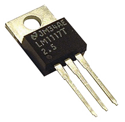
PDF LM1117 Data sheet ( Hoja de datos )
| Número de pieza | LM1117 | |
| Descripción | 800mA Low-Dropout Linear Regulator | |
| Fabricantes | National Semiconductor | |
| Logotipo | ||
 1. Datasheet - 800mA Linear Regulator Hay una vista previa y un enlace de descarga de LM1117 (archivo pdf) en la parte inferior de esta página. Total 21 Páginas | ||
|
No Preview Available !
April 2006
LM1117/LM1117I
800mA Low-Dropout Linear Regulator
General Description
The LM1117 is a series of low dropout voltage regulators
with a dropout of 1.2V at 800mA of load current. It has the
same pin-out as National Semiconductor’s industry standard
LM317.
The LM1117 is available in an adjustable version, which can
set the output voltage from 1.25V to 13.8V with only two
external resistors. In addition, it is also available in five fixed
voltages, 1.8V, 2.5V, 2.85V, 3.3V, and 5V.
The LM1117 offers current limiting and thermal shutdown. Its
circuit includes a zener trimmed bandgap reference to as-
sure output voltage accuracy to within ±1%.
The LM1117 series is available in LLP, TO-263, SOT-223,
TO-220, and TO-252 D-PAK packages. A minimum of 10µF
tantalum capacitor is required at the output to improve the
transient response and stability.
Features
n Available in 1.8V, 2.5V, 2.85V, 3.3V, 5V, and Adjustable
Versions
n Space Saving SOT-223 and LLP Packages
n Current Limiting and Thermal Protection
n Output Current
800mA
n Line Regulation
0.2% (Max)
n Load Regulation
0.4% (Max)
n Temperature Range
— LM1117
0˚C to 125˚C
— LM1117I
−40˚C to 125˚C
Applications
n 2.85V Model for SCSI-2 Active Termination
n Post Regulator for Switching DC/DC Converter
n High Efficiency Linear Regulators
n Battery Charger
n Battery Powered Instrumentation
Typical Application
Active Terminator for SCSI-2 Bus
Fixed Output Regulator
10091905
© 2006 National Semiconductor Corporation DS100919
10091928
www.national.com
1 page 
LM1117 Electrical Characteristics (Continued)
Typicals and limits appearing in normal type apply for TJ = 25˚C. Limits appearing in Boldface type apply over the entire junc-
tion temperature range for operation, 0˚C to 125˚C.
Symbol
Parameter
Conditions
Min
(Note 5)
Typ
(Note 4)
Max
(Note 5)
Units
∆VOUT
Load Regulation
(Note 6)
VIN-V OUT Dropout Voltage
(Note 7)
ILIMIT
Current Limit
Minimum Load
Current (Note 8)
Quiescent Current
Thermal Regulation
Ripple Regulation
Adjust Pin Current
LM1117-ADJ
VIN-VOUT = 3V, 10 ≤ IOUT ≤ 800mA
LM1117-1.8
VIN = 3.2V, 0 ≤ IOUT ≤ 800mA
LM1117-2.5
VIN = 3.9V, 0 ≤ IOUT ≤ 800mA
LM1117-2.85
VIN = 4.25V, 0 ≤ IOUT ≤ 800mA
LM1117-3.3
VIN = 4.75V, 0 ≤ IOUT ≤ 800mA
LM1117-5.0
VIN = 6.5V, 0 ≤ IOUT ≤ 800mA
IOUT = 100mA
IOUT = 500mA
IOUT = 800mA
VIN-VOUT = 5V, TJ = 25˚C
LM1117-ADJ
VIN = 15V
LM1117-1.8
VIN ≤ 15V
LM1117-2.5
VIN ≤ 15V
LM1117-2.85
VIN ≤ 10V
LM1117-3.3
VIN ≤ 15V
LM1117-5.0
VIN ≤ 15V
TA = 25˚C, 30ms Pulse
fRIPPLE =1 20Hz, VIN-VOUT = 3V VRIPPLE
= 1VPP
800
60
0.2 0.4 %
1 10 mV
1 10 mV
1
1
1
1.10
1.15
1.20
1200
1.7
5
5
10
10
15
1.20
1.25
1.30
1500
5
10
10
mV
mV
mV
V
V
V
mA
mA
mA
mA
5 10 mA
5 10 mA
5 10 mA
0.01 0.1 %/W
75 dB
60 120 µA
Adjust Pin Current
Change
Temperature Stability
10 ≤ IOUT≤ 800mA,
1.4V ≤ VIN-VOUT ≤ 10V
0.2 5 µA
0.5 %
Long Term Stability
RMS Output Noise
Thermal Resistance
Junction-to-Case
TA = 125˚C, 1000Hrs
(% of VOUT), 10Hz ≤ f ≤10kHz
3-Lead SOT-223
3-Lead TO-220
0.3
0.003
15.0
3.0
%
%
˚C/W
˚C/W
3-Lead TO-252
10 ˚C/W
Thermal Resistance
Junction-to-Ambient
(No air flow)
3-Lead SOT-223 (No heat sink)
3-Lead TO-220 (No heat sink)
3-Lead TO-252 (Note 9) (No heat sink)
136 ˚C/W
79 ˚C/W
92 ˚C/W
3-Lead TO-263
55 ˚C/W
8-Lead LLP(Note 10)
40 ˚C/W
5 www.national.com
5 Page 
Application Note (Continued)
10091937
FIGURE 5. Cross-sectional view of Integrated Circuit
Mounted on a printed circuit board. Note that the case
temperature is measured at the point where the leads
contact with the mounting pad surface
The LM1117 regulators have internal thermal shutdown to
protect the device from over-heating. Under all possible
operating conditions, the junction temperature of the LM1117
must be within the range of 0˚C to 125˚C. A heatsink may be
required depending on the maximum power dissipation and
maximum ambient temperature of the application. To deter-
mine if a heatsink is needed, the power dissipated by the
regulator, PD , must be calculated:
IIN = IL + IG
PD = (VIN-VOUT)I L + VINIG
Figure 6 shows the voltages and currents which are present
in the circuit.
The next parameter which must be calculated is the maxi-
mum allowable temperature rise, TR(max):
TR(max) = TJ(max)-TA(max)
where TJ(max) is the maximum allowable junction tempera-
ture (125˚C), and TA(max) is the maximum ambient tem-
perature which will be encountered in the application.
Using the calculated values for TR(max) and PD, the maxi-
mum allowable value for the junction-to-ambient thermal
resistance (θJA) can be calculated:
θJA = TR(max)/PD
If the maximum allowable value for θJA is found to be
≥136˚C/W for SOT-223 package or ≥79˚C/W for TO-220
package or ≥92˚C/W for TO-252 package, no heatsink is
needed since the package alone will dissipate enough heat
to satisfy these requirements. If the calculated value for θJA
falls below these limits, a heatsink is required.
As a design aid, Table 1 shows the value of the θJA of
SOT-223 and TO-252 for different heatsink area. The copper
patterns that we used to measure these θJAs are shown at
the end of the Application Notes Section. Figure 7 and Figure
8 reflects the same test results as what are in the Table 1
Figure 9 and Figure 10 shows the maximum allowable power
dissipation vs. ambient temperature for the SOT-223 and
TO-252 device. Figures Figure 11 and Figure 12 shows the
maximum allowable power dissipation vs. copper area (in2)
for the SOT-223 and TO-252 devices. Please see AN1028
for power enhancement techniques to be used with SOT-223
and TO-252 packages.
*Application Note AN-1187 discusses improved thermal per-
formance and power dissipation for the LLP.
10091916
FIGURE 6. Power Dissipation Diagram
Layout
1
2
3
4
5
6
7
8
9
10
11
12
13
TABLE 1. θJA Different Heatsink Area
Copper Area
Thermal Resistance
Top Side (in2)*
0.0123
Bottom Side (in2)
0
(θJA,˚C/W) SOT-223
136
(θJA,˚C/W) TO-252
103
0.066
0
123
87
0.3 0
84
60
0.53
0
75
54
0.76
0
69
52
1 0 66
47
0 0.2 115
84
0 0.4 98
70
0 0.6 89
63
0 0.8 82
57
0 1 79
57
0.066
0.066
125
89
0.175
0.175
93
72
11 www.national.com
11 Page | ||

| Páginas | Total 21 Páginas | |
| PDF Descargar | [ Datasheet LM1117.PDF ] | |
Hoja de datos destacado
| Número de pieza | Descripción | Fabricantes |
| LM111 | Voltage Comparator | National Semiconductor |
| LM111 | Voltage comparator | NXP Semiconductors |
| LM111 | VOLTAGE COMPARATORS | STMicroelectronics |
| LM111 | Voltage comparator | NXP Semiconductors |
| Número de pieza | Descripción | Fabricantes |
| SLA6805M | High Voltage 3 phase Motor Driver IC. |
Sanken |
| SDC1742 | 12- and 14-Bit Hybrid Synchro / Resolver-to-Digital Converters. |
Analog Devices |
|
DataSheet.es es una pagina web que funciona como un repositorio de manuales o hoja de datos de muchos de los productos más populares, |
| DataSheet.es | 2020 | Privacy Policy | Contacto | Buscar |