|
|
|
PDF LM27964 Data sheet ( Hoja de datos )
| Número de pieza | LM27964 | |
| Descripción | White LED Driver System | |
| Fabricantes | National Semiconductor | |
| Logotipo | ||
Hay una vista previa y un enlace de descarga de LM27964 (archivo pdf) en la parte inferior de esta página. Total 14 Páginas | ||
|
No Preview Available !
August 2007
LM27964
White LED Driver System with I2C Compatible Brightness
Control
General Description
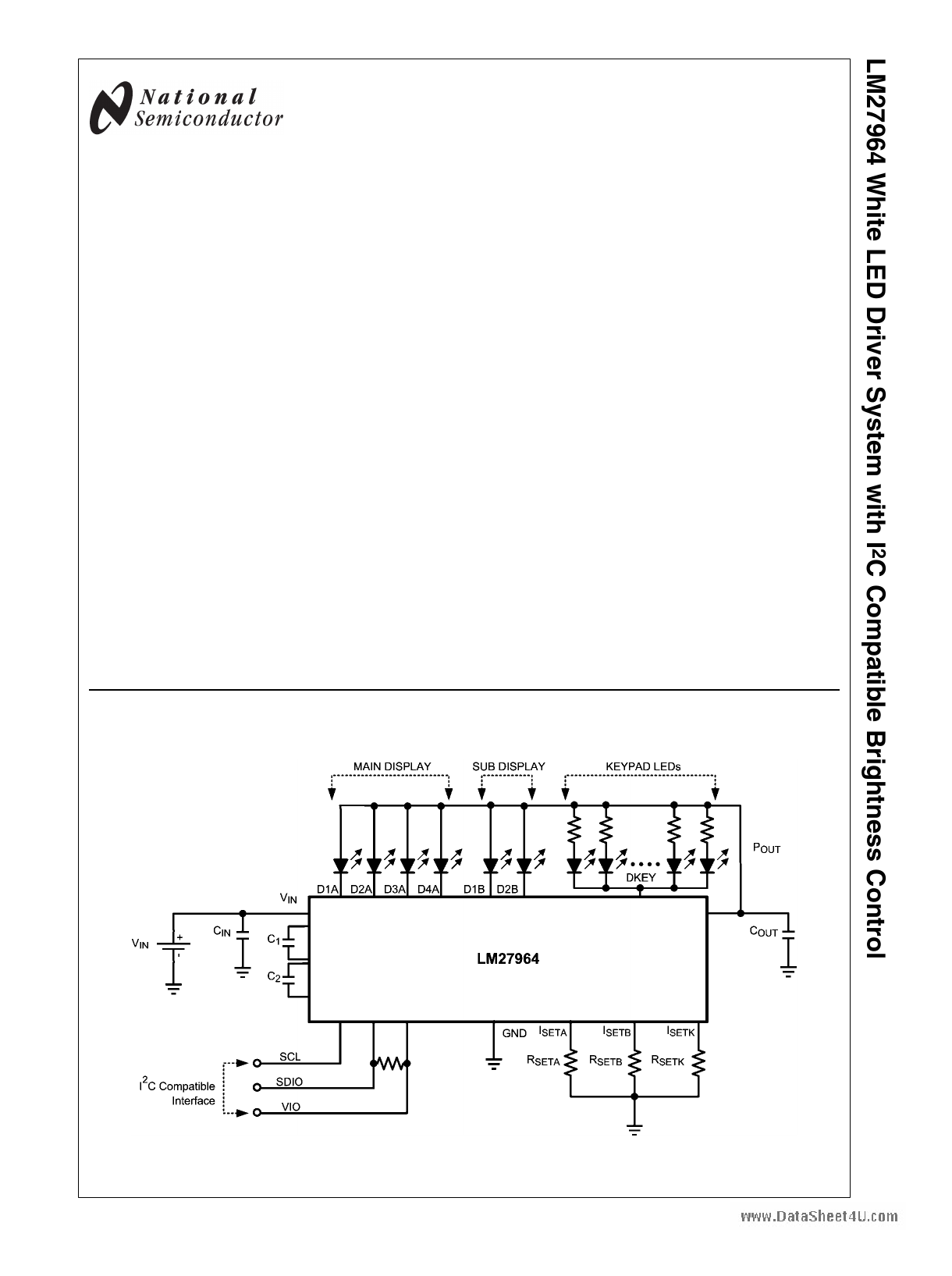
The LM27964 is a charge-pump-based white-LED driver that
is ideal for mobile phone display backlighting. The LM27964
can drive up to 6 LEDs in parallel along with multiple keypad
LEDs, with a total output current up to 180mA. Regulated in-
ternal current sources deliver excellent current matching in all
www.DataSheeLt4EUD.cso. m
The LED driver current sources are split into two indepen-
dently controlled groups. The primary group (4 LEDs) can be
used to backlight the main phone display and the second
group (2 LEDs) can be used to backlight a secondary display.
A single Keypad LED driver can power up to 16 keypad LEDs
with a current of 5mA each. The LM27964 has an I2C com-
patible interface that allows the user to independently control
the brightness on each bank of LEDs.
The LM27964 works off an extended Li-Ion input voltage
range (2.7V to 5.5V). The device provides excellent efficiency
without the use of an inductor by operating the charge pump
in a gain of 3/2, or in Pass-Mode. The proper gain for main-
taining current regulation is chosen, based on LED forward
voltage, so that efficiency is maximized over the input voltage
range.
The LM27964 is available in National's small 24-pin Leadless
Leadframe Package (LLP-24).
Features
■ 87% Peak LED Drive Efficiency
■ 0.2% Current Matching between Current Sinks
■ Drives 6 LEDs with up to 30mA per LED in two distinct
groups, for backlighting two displays (main LCD and sub
LCD)
■ Dedicated Keypad LED Driver with up to 80mA of drive
current
■ Independent Resistor-Programmable Current Settings
■ I2C Compatible Brightness Control Interface
■ Adaptive 1×- 3/2× Charge Pump
■ Extended Li-Ion Input: 2.7V to 5.5V
■ Small low profile industry standard leadless package, LLP
24 : (4mm x 4mm x 0.8mm)
■ LM27964SQ-I LED PWM frequency = 10kHz,
LM27964SQ-C LED PWM frequency = 23kHz
Applications
■ Mobile Phone Display Lighting
■ Mobile Phone Keypad Lighting
■ PDAs Backlighting
■ General LED Lighting
Typical Application Circuit
© 2007 National Semiconductor Corporation 201381
20138101
www.national.com
1 page 
Note 7: Junction-to-ambient thermal resistance is highly dependent on application and board layout. In applications where high maximum power dissipation
exists, special care must be paid to thermal dissipation issues in board design. For more information, please refer to National Semiconductor Application Note
1187: Leadless Leadframe Package (AN-1187).
Note 8: Min and Max limits are guaranteed by design, test, or statistical analysis. Typical numbers are not guaranteed, but do represent the most likely norm.
Note 9: CIN, CPOUT, C1, and C2 : Low-ESR Surface-Mount Ceramic Capacitors (MLCCs) used in setting electrical characteristics
Note 10: The maximum total output current for the LM27964 should be limited to 180mA. The total output current can be split among any of the three banks
(IDxA = IDxB = 30mA Max., IDKEY = 80mA Max.). Under maximum output current conditions, special attention must be given to input voltage and LED forward
voltage to ensure proper current regulation. See the Maximum Output Current section of the datasheet for more information.
Note 11: For each IDxx output pin, headroom voltage is the voltage across the internal current sink connected to that pin. For Group A and B outputs, VHR =
VOUT -VDxx. If headroom voltage requirement is not met, LED current regulation will be compromised.
Note 12: For the two groups of outputs on a part (BankA and BankB), the following are determined: the maximum output current in the group (MAX), the minimum
output current in the group (MIN), and the average output current of the group (AVG). For each group, two matching numbers are calculated: (MAX-AVG)/AVG
and (AVG-MIN)/AVG. The largest number of the two (worst case) is considered the matching figure for the bank. The matching figure for a given part is considered
to be the highest matching figure of the two banks. The typical specification provided is the most likely norm of the matching figure for all parts.
Note 13: SCL and SDIO should be glitch-free in order for proper brightness control to be realized.
Block Diagram
www.DataSheet4U.com
20138103
5 www.national.com
5 Page 
forward voltage. Excessive power dissipation may also limit
output current capability of an application.
Total Output Current Capability
The maximum output current that can be drawn from the
LM27964 is 180mA. Each driver bank has a maximum allotted
current per Dxx sink that must not be exceeded.
DRIVER TYPE
MAXIMUM Dxx CURRENT
DxA 30mA per DxA Pin
DxB 30mA per DxB Pin
DKEY
80mA
The 180mA load can be distributed in many different config-
urations. Special care must be taken when running the
LM27964 at the maximum output current to ensure proper
functionality.
www.DataPSAheReAt4LUL.EcoLmCONNECTED OUTPUTS
Outputs D1A-4A or D1B-D2B may be connected together to
drive one or two LEDs at higher currents. In such a configu-
ration, all four parallel current sinks (BankA) of equal value
can drive a single LED. The LED current programmed for
BankA should be chosen so that the current through each of
the outputs is programmed to 25% of the total desired LED
current. For example, if 60mA is the desired drive current for
a single LED, RSETA should be selected such that the current
through each of the current sink inputs is 15mA. Similarly, if
two LEDs are to be driven by pairing up the D1A-4A inputs
(i.e D1A-2A, D3A-4A), RSETA should be selected such that the
current through each current sink input is 50% of the desired
LED current. The same RSETx selection guidelines apply to
BankB diodes.
Connecting the outputs in parallel does not affect internal op-
eration of the LM27964 and has no impact on the Electrical
Characteristics and limits previously presented. The available
diode output current, maximum diode voltage, and all other
specifications provided in the Electrical Characteristics table
apply to this parallel output configuration, just as they do to
the standard 4-LED application circuit.
Both BankA and BankB utilize LED forward voltage sensing
circuitry on each Dxx pin to optimize the charge-pump gain
for maximum efficiency. Due to the nature of the sensing cir-
cuitry, it is not recommended to leave any of the DxA or DxB
pins unused if either diode bank is going to be used during
normal operation. Leaving DxA and/or DxB pins unconnected
will force the charge-pump into 3/2× mode over the entire
VIN range negating any efficiency gain that could be achieve
by switching to 1× mode at higher input voltages.
Care must be taken when selecting the proper RSETx value.
The current on any Dxx pin must not exceed the maximum
current rating for any given current sink pin.
POWER EFFICIENCY
Efficiency of LED drivers is commonly taken to be the ratio of
power consumed by the LEDs (PLED) to the power drawn at
the input of the part (PIN). With a 1.5x/1x charge pump, the
input current is equal to the charge pump gain times the output
current (total LED current). The efficiency of the LM27964 can
be predicted as follows:
PLEDTOTAL = (VLEDA × NA × ILEDA) +
(VLEDB × NB × ILEDB) + (VLEDK × NK × ILEDK)
PIN = VIN × IIN
PIN = VIN × (GAIN × ILEDTOTAL + IQ)
E = (PLEDTOTAL ÷ PIN)
It is also worth noting that efficiency as defined here is in part
dependent on LED voltage. Variation in LED voltage does not
affect power consumed by the circuit and typically does not
relate to the brightness of the LED. For an advanced analysis,
it is recommended that power consumed by the circuit (VIN x
IIN) be evaluated rather than power efficiency.
POWER DISSIPATION
The power dissipation (PDISS) and junction temperature (TJ)
can be approximated with the equations below. PIN is the
power generated by the 1.5x/1x charge pump, PLED is the
power consumed by the LEDs, TA is the ambient temperature,
and θJA is the junction-to-ambient thermal resistance for the
LLP-24 package. VIN is the input voltage to the LM27964,
VLED is the nominal LED forward voltage, N is the number of
LEDs and ILED is the programmed LED current.
PDISS = PIN - PLEDA - PLEDB - PLEDK
PDISS= (GAIN × VIN × ILEDA + LEDB + LEDK) - (VLEDA × NA ×
ILEDA) -
(VLEDB × NB × ILEDB) - (VLEDK × NK × ILEDK)
TJ = TA + (PDISS x θJA)
The junction temperature rating takes precedence over the
ambient temperature rating. The LM27964 may be operated
outside the ambient temperature rating, so long as the junc-
tion temperature of the device does not exceed the maximum
operating rating of 100°C. The maximum ambient tempera-
ture rating must be derated in applications where high power
dissipation and/or poor thermal resistance causes the junc-
tion temperature to exceed 100°C.
THERMAL PROTECTION
Internal thermal protection circuitry disables the LM27964
when the junction temperature exceeds 170°C (typ.). This
feature protects the device from being damaged by high die
temperatures that might otherwise result from excessive pow-
er dissipation. The device will recover and operate normally
when the junction temperature falls below 165°C (typ.). It is
important that the board layout provide good thermal conduc-
tion to keep the junction temperature within the specified
operating ratings.
CAPACITOR SELECTION
The LM27964 requires 4 external capacitors for proper oper-
ation (C1 = C2 = 1µF, CIN = COUT = 2.2µF). Surface-mount
multi-layer ceramic capacitors are recommended. These ca-
pacitors are small, inexpensive and have very low equivalent
series resistance (ESR <20mΩ typ.). Tantalum capacitors,
OS-CON capacitors, and aluminum electrolytic capacitors are
not recommended for use with the LM27964 due to their high
ESR, as compared to ceramic capacitors.
For most applications, ceramic capacitors with X7R or X5R
temperature characteristic are preferred for use with the
LM27964. These capacitors have tight capacitance tolerance
(as good as ±10%) and hold their value over temperature
(X7R: ±15% over -55°C to 125°C; X5R: ±15% over -55°C to
85°C).
Capacitors with Y5V or Z5U temperature characteristic are
generally not recommended for use with the LM27964. Ca-
pacitors with these temperature characteristics typically have
wide capacitance tolerance (+80%, -20%) and vary signifi-
cantly over temperature (Y5V: +22%, -82% over -30°C to
+85°C range; Z5U: +22%, -56% over +10°C to +85°C range).
Under some conditions, a nominal 1µF Y5V or Z5U capacitor
could have a capacitance of only 0.1µF. Such detrimental de-
viation is likely to cause Y5V and Z5U capacitors to fail to
11 www.national.com
11 Page | ||
| Páginas | Total 14 Páginas | |
| PDF Descargar | [ Datasheet LM27964.PDF ] | |
Hoja de datos destacado
| Número de pieza | Descripción | Fabricantes |
| LM2796 | Dual-Display White LED Driver with 3/2x Switched Capacitor Boost | National Semiconductor |
| LM2796 | LM2796 Dual-Display White LED Driver with 3/2x Switched Capacitor Boost (Rev. A) | Texas Instruments |
| LM27961 | LM27961 Dual-Display White LED Driver with 3/2x Switched Capacitor Boost (Rev. A) | Texas Instruments |
| LM27961 | Dual-Display White | National Semiconductor |
| Número de pieza | Descripción | Fabricantes |
| SLA6805M | High Voltage 3 phase Motor Driver IC. |
Sanken |
| SDC1742 | 12- and 14-Bit Hybrid Synchro / Resolver-to-Digital Converters. |
Analog Devices |
|
DataSheet.es es una pagina web que funciona como un repositorio de manuales o hoja de datos de muchos de los productos más populares, |
| DataSheet.es | 2020 | Privacy Policy | Contacto | Buscar |